Semiconductor & IC packaging materials Market

Semiconductor & IC packaging materials Market by Type (Organic substrate, Bonding wires, Leadframes, Encapsulation resins, Ceramic packages, Die attach materials, Solder balls), Packaging Technology, End-use industry, and Region - Global Forecast to 2029

Report Code: CH 2348 Mar, 2024, by marketsandmarkets.com

The semiconductor & IC packaging materials market is projected to reach USD 70.9 billion by 2029, at a CAGR of 10.1% from USD 43.9 billion in 2024. The market growth is driven by increasing demand from consumer electronics industry, growing miniaturization and densification in the electronic sector and adoption of emerging technologies like  5G and autonomous vehicles.

Semiconductor & IC packaging materials Market

To know about the assumptions considered for the study, Request for Free Sample Report

Attractive Opportunities in the Semiconductor & IC Packaging Materials Market

Semiconductor & IC packaging materials Market

Market Dynamics

Driver: Increasing demand from consumer electronics market

The semiconductor and IC packaging material industry is propelled forward by the rising demand from the consumer electronics sector, including smartphones, tablets, laptops, and smartwatches, which heavily rely on semiconductor chips and integrated circuits (ICs) for their functionalities. As consumers seek more compact, faster, and feature-rich electronic products, there's a surge in the need for advanced semiconductor components and packaging materials. This demand surge is driven by factors such as miniaturization and integration of functions, heightened performance expectations, the growth of IoT and connected devices, advancements in display and sensor technologies, and the expanding global market for consumer electronics. These drivers collectively fuel innovation, technological progress, and market expansion within the semiconductor and IC packaging material industry, positioning it as a pivotal player in the evolving landscape of consumer electronics.

Driver: Growing miniaturization and densification in the electronic sector.

The growing trend of miniaturization and densification in the electronics sector is a significant driver for the semiconductor and IC packaging materials market. As electronic devices become smaller and more compact, manufacturers face challenges in integrating complex functionalities into limited space. This trend is particularly evident in consumer electronics like smartphones, wearables, and IoT devices, where consumers demand sleek designs without compromising performance. To address these challenges, semiconductor manufacturers are developing advanced chips with higher integration levels, packing more functionalities into smaller components. This trend drives the need for innovative packaging materials that can accommodate these complex chip designs while ensuring reliability, performance, and thermal management. IC packaging materials play a crucial role in enabling miniaturization by providing electrical insulation, mechanical support, thermal dissipation, and signal integrity within the compact space of semiconductor packages. Materials such as organic substrates, leadframes, encapsulation resins, and thermal interface materials are designed to meet the stringent requirements of miniaturized electronics, offering solutions for compact yet efficient packaging solutions. Furthermore, densification in the electronics sector, where more components are packed into smaller areas, increases the demand for advanced packaging materials capable of handling higher pin densities, complex interconnections, and stringent reliability standards. Overall, the trend of miniaturization and densification drives continuous innovation and growth in the semiconductor and IC packaging materials market to meet the evolving needs of the electronics industry.

Driver: Adoption of emerging technologies like 5G and autonomous vehicles.

The adoption of emerging technologies such as 5G and autonomous vehicles is a significant driver for the semiconductor and IC packaging materials market. 5G technology requires high-performance semiconductor chips and advanced packaging materials to support ultra-fast data processing, low-latency communication, and increased connectivity. This drives demand for materials with superior thermal management, signal integrity, and electrical insulation properties. Similarly, autonomous vehicles rely heavily on semiconductor components and ICs for functions like sensors, data processing, and connectivity. Advanced packaging materials are essential to ensure the reliability, durability, and performance of these semiconductor components in harsh automotive environments. As the adoption of 5G and autonomous vehicles continues to grow, the demand for specialized semiconductor and IC packaging materials will increase, driving innovation and growth in the market.

Restraint: IP concerns in the semiconductor industry during outsourcing & testing process

IP concerns in the semiconductor industry during outsourcing and testing processes are a major restraint for the semiconductor and IC packaging materials market. When semiconductor companies outsource manufacturing or testing processes to third-party vendors, there is a risk of intellectual property (IP) theft or leakage. This risk can arise from sharing sensitive design information, manufacturing processes, or proprietary technologies with external partners. Such concerns can hinder collaboration and innovation in the semiconductor industry, leading to reluctance in adopting advanced packaging materials that may involve sharing confidential IP with vendors. Additionally, stringent regulations and legal complexities surrounding IP protection further exacerbate these concerns, impacting the willingness of semiconductor companies to engage in outsourcing and testing activities. As a result, IP concerns act as a significant barrier, limiting market growth and innovation in semiconductor and IC packaging materials.

Restraint: Technological change and obsolescence

Technological change and obsolescence pose significant restraints for the semiconductor and IC packaging market. Rapid technological advancements lead to frequent upgrades and changes in semiconductor designs, functionalities, and packaging requirements. This dynamic environment increases the risk of product obsolescence, where existing packaging solutions may become outdated or incompatible with newer semiconductor technologies. Moreover, the pace of technological change often outpaces the development of corresponding packaging materials, creating challenges in meeting evolving performance, miniaturization, and functionality demands. Semiconductor companies face the dilemma of investing in costly packaging solutions that may quickly become obsolete or adopting interim solutions that may not fully align with future technology trends. Additionally, managing the transition from older packaging technologies to newer ones requires significant time, resources, and investment, further complicating the market landscape. These factors collectively contribute to technological change and obsolescence acting as restraints for the semiconductor and IC packaging market, impacting market growth and innovation.

Opportunity: Integration with advanced technologies

Integration with advanced technologies presents a significant opportunity for the semiconductor and IC packaging materials market. As industries adopt cutting-edge technologies like artificial intelligence (AI), machine learning (ML), 5G connectivity, Internet of Things (IoT), and autonomous systems, the demand for high-performance semiconductor components and advanced packaging materials increases. These technologies require sophisticated packaging solutions to meet stringent performance, reliability, and thermal management requirements. For example, AI and ML applications demand chips with high computing power and efficient heat dissipation, driving the need for innovative packaging materials that can handle these demands. Similarly, the rollout of 5G networks and the proliferation of IoT devices require semiconductor packages capable of supporting high-speed data transmission, low-latency communication, and connectivity across diverse devices. Advanced packaging materials play a crucial role in enabling these capabilities, creating opportunities for companies specializing in semiconductor and IC packaging materials to innovate and capture a growing market segment.

Challenge: The high cost of advanced materials.

The high cost of advanced materials presents a significant challenge for the semiconductor and IC packaging materials market. Developing and manufacturing cutting-edge materials with enhanced performance, reliability, and functionality often involves substantial research and development (R&D) investments, as well as specialized production processes. These factors contribute to higher production costs, which can be passed on to semiconductor companies and end-users, making advanced packaging materials less cost-effective compared to traditional alternatives. Furthermore, the semiconductor industry operates in a highly competitive and cost-sensitive environment, where companies are constantly seeking ways to reduce production costs and improve profit margins. The high initial investment required for adopting advanced materials may deter some companies, particularly smaller players, from embracing these technologies, leading to slower adoption rates and limited market penetration. Balancing the benefits of advanced materials with cost considerations remains a key challenge for the semiconductor and IC packaging materials market.

Market Ecosystem

A market ecosystem for semiconductor & IC packaging materials refers to the interconnected network of various entities, factors, and dynamics that collectively influence the production, distribution, and consumption of semiconductor & IC packaging materials in the market. This ecosystem involves a range of participants, both internal and external, and includes various components that interact with each other to shape the overall functioning of the market. The key players in the market are LG Chem Ltd. (South Korea), Jiangsu ChangJian Technology Co., Ltd. (China), Henkel AG & Co. KGaA (Germany), Kyocera Corporation (Japan), ASE (Taiwan), Siliconware Precision Industries Co., Ltd. (Taiwan), Amkor Technology (US), Texas Instruments (US), IBIDEN CO., LTD. (Japan), Powertech Technology Inc. (Taiwan)  etc.

Semiconductor & IC Packaging Materials Market: Ecosystem

Semiconductor & IC packaging materials Market Ecosystem

Source: Secondary Research, Interviews with Experts, and MarketsandMarkets Analysis

"Organic substrate is the largest sub-segment amongst the type segment in the semiconductor & IC packaging materials market in 2024, in terms of value."

The dominance of organic substrates in the semiconductor and IC packaging materials market stems from several key advantages. These substrates, typified by printed circuit boards (PCBs), offer a cost-effective solution crucial for mass production, aligning with the industry's push for economies of scale. Their excellent electrical insulation properties prevent shorts and maintain signal integrity, while their versatility allows for complex designs and component integration, catering to diverse semiconductor applications. Additionally, their lightweight nature aids in system miniaturization and device portability. Furthermore, their compatibility with standard PCB fabrication processes ensures faster production cycles and reduced time-to-market. Advancements like high-speed laminate materials and low-loss dielectrics have bolstered their performance in signal transmission and thermal management, making organic substrates the preferred choice in modern semiconductor packaging, underscored by their cost-effectiveness, insulation, design flexibility, lightweight build, ease of manufacturing, and continual technological enhancements.

“Small  outline package (SOP) accounted for the largest by packaging technology share of the semiconductor & IC packaging materials market in 2024” in terms of value.

Small Outline Package (SOP) technology dominates the semiconductor and IC packaging materials market due to its numerous advantages. SOPs are prized for their compactness and low profile, making them perfect for space-constrained applications like mobile devices, wearables, and IoT gadgets. This compact design not only saves material but also reduces package weight, aligning well with industries focused on lightweight and portable electronics. Moreover, SOPs feature a small lead pitch, allowing for higher pin density and seamless integration of semiconductor components, enhancing functionality within a smaller space. Their compatibility with surface mount technology (SMT) enables automated assembly processes, boosting production efficiency and lowering manufacturing costs. This SMT compatibility also improves thermal management by facilitating direct mounting on PCBs, leading to better heat dissipation and device reliability. SOP technology's versatility is evident in various package configurations like SOP-8, SOP-16, and SOP-28, catering to diverse semiconductor applications. Furthermore, SOPs deliver excellent electrical performance with low parasitic capacitance and inductance, crucial for high-speed digital and analog operations. They also offer robust protection against environmental elements such as moisture and mechanical stress, ensuring semiconductor devices' durability and reliability. In essence, SOP technology's compactness, high pin density, SMT compatibility, thermal management capabilities, versatility, and electrical performance collectively establish it as the top choice in the semiconductor and IC packaging materials market.

“Consumer electronics accounted for the largest end-use industry for the semiconductor & IC packaging materials market, in terms of value in 2024”

The dominance of consumer electronics in the semiconductor and IC packaging materials market is driven by several key factors. Firstly, the industry's widespread use of semiconductor devices and ICs in products like smartphones, tablets, laptops, gaming consoles, smart TVs, and wearables fuels the demand for advanced packaging solutions that meet performance, miniaturization, and functionality requirements. Secondly, the rapid innovation in consumer electronics demands packaging materials that support cutting-edge technologies such as high-speed data processing, AI, AR, and IoT connectivity. Semiconductor packaging materials are essential for providing electrical insulation, thermal management, signal integrity, and mechanical protection to these components. Additionally, the industry's focus on cost-effective solutions, fast time-to-market, and efficient assembly processes drives the adoption of materials like organic substrates, leadframes, encapsulation resins, and advanced die attach materials. The global adoption of consumer electronics drives large-scale production volumes and economies of scale, leading to cost reductions and packaging technology advancements to meet diverse consumer preferences for sleek, lightweight, energy-efficient devices.

"Asia pacific is the largest market for semiconductor & IC packaging materials Market in 2024, in terms of value."

Asia Pacific stands out as the foremost market for semiconductor and IC packaging materials, driven by various factors that underscore its industry dominance. The region hosts major electronics manufacturing hubs like China, Japan, South Korea, Taiwan, and Singapore, boasting robust semiconductor ecosystems with a comprehensive presence of foundries, packaging facilities, equipment suppliers, and research institutions. This integration creates a highly competitive market environment, fostering continuous innovation and technological advancement, particularly evident in countries like South Korea and Japan renowned for their leadership in semiconductor research and manufacturing. The relentless pursuit of technological excellence propels the demand for high-performance packaging materials capable of meeting the exacting standards of advanced semiconductor devices. Asia Pacific's thriving consumer electronics market further propels this demand, fueled by rising disposable incomes, urbanization, and digitalization trends. This market encompasses a wide array of products such as smartphones, tablets, laptops, smart home devices, wearables, and automotive electronics, all heavily reliant on semiconductor and IC packaging materials for their functionality and performance. The region's strategic position as a global manufacturing hub provides additional advantages, including cost-effectiveness, efficient supply chains, and access to skilled labor. Major semiconductor manufacturers, assembly, and testing facilities, as well as equipment suppliers, bolster Asia Pacific's status as a pivotal market for semiconductor packaging materials. Government initiatives, investment incentives, and favorable business environments further stimulate industry growth and attract foreign investments, contributing significantly to the expansion of the semiconductor and IC packaging materials market in Asia Pacific. Overall, Asia Pacific's leadership in semiconductor manufacturing, technological innovation, growing consumer electronics demand, manufacturing efficiencies, and supportive business climates collectively position it as the largest and most dynamic market for semiconductor and IC packaging materials worldwide.

Semiconductor & IC packaging materials Market by Region

To know about the assumptions considered for the study, download the pdf brochure

Key Market Players

The key players in this market are LG Chem Ltd. (South Korea), Jiangsu ChangJian Technology Co., Ltd. (China), Henkel AG & Co. KGaA (Germany), Kyocera Corporation (Japan), ASE (Taiwan), Siliconware Precision Industries Co., Ltd. (Taiwan), Amkor Technology (US), Texas Instruments (US), IBIDEN CO., LTD. (Japan), Powertech Technology Inc. (Taiwan)  etc. Continuous developments in the market—including new product launches, mergers & acquisitions, agreements, and expansions—are expected to help the market grow. Leading manufacturers of semiconductor & IC packaging materials have opted for new product launches to sustain their market position.

Get online access to the report on the World's First Market Intelligence Cloud

  • Easy to Download Historical Data & Forecast Numbers
  • Company Analysis Dashboard for high growth potential opportunities
  • Research Analyst Access for customization & queries
  • Competitor Analysis with Interactive dashboard
  • Latest News, Updates & Trend analysis
Request Sample

Scope of the Report

Report Metric

Details

Years considered for the study

2020-2029

Base Year

2023

Forecast period

2024–2029

Units considered

Value (USD Billion/Million)

Segments

Type, Packaging technology, End-use industry and Region

Regions

Asia Pacific, North America, Europe, Middle East & Africa, and South America

Companies

LG Chem Ltd. (South Korea), Jiangsu ChangJian Technology Co., Ltd. (China), Henkel AG & Co. KGaA (Germany), Kyocera Corporation (Japan), ASE (Taiwan), Siliconware Precision Industries Co., Ltd. (Taiwan), Amkor Technology (US), Texas Instruments (US), IBIDEN CO., LTD. (Japan), Powertech Technology Inc. (Taiwan)

Segmentation

This report categorizes the global Semiconductor & IC packaging materials market based on type, packaging technology, end-use industry and region.

On the basis of type, the market has been segmented as follows:
  • Organic substrate
  • Bonding wires
  • Leadframes
  • Encapsulation resins
  • Ceramic packages
  • Die attach materials
  • Thermal interface materials
  • Solder balls
  • Others
On the basis of packaging technology, the market has been segmented as follows:
  • Small outline package (SOP)
  • Grid array (GA)
  • Quad flat no-leads (QFN)
  • Dual Flat No-leads (DFN)
  • Quad flat packages (QFP)
  • Dual-in-line (DIP)
  • Others
On the basis of end-use industry, the market has been segmented as follows:
  • Consumer electronics
  • Automotive
  • Aerospace & defense
  • IT & telecommunication
  • Healthcare
  • Othersl
On the basis of region, the market has been segmented as follows:
  • North America
  • Europe
  • Asia Pacific
  • Middle East & Africa
  • South America

Recent Developments

  • In March 2024, Kyocera Corporation (Japan), under the leadership of President Hideo Tanimoto, has revealed plans to integrate its existing Shiga Yohkaichi Plant located in Hebimizo-cho, Higashiomi, Shiga, and Shiga Gamo Plant situated in Kawai-cho, Higashiomi, Shiga. This integration aims to bolster operational efficiency, and consequently, the combined entity will be rebranded as the "Shiga Higashiomi Plant." Effective from April 1, 2024, the plant will commence operations under its new name, with no alterations to its physical location.
  • In November 2023, Amkor Technology (US) a leading provider of semiconductor packaging and test services, has announced its plan to build an advanced packaging and test facility in Peoria, Arizona. By the time of full project completion, Amkor projects to invest approximately $2 billion and employ approximately 2,000 people at the new facility.
  • In June 2023, Henkel AG & Co. AGaA (Germany) has emphasized the significance of India as a key market, highlighting the company's ongoing commitment to invest in laboratory infrastructure and enhance capacity, particularly within the electronics sector. Additionally, Knobel recently inaugurated the Inspiration Centre Dusseldorf (ICD), a project that represents an investment of 130 million euros (USD 141.2 million), demonstrating Henkel's dedication to fostering innovation and growth.
  • In February 2023, LG Chem Ltd. (South Korea) entered into  an offtake agreement with Piedmont Lithium, Inc. (US) for 200,000 metric tons of SC6. Starting in the third quarter of 2023, Piedmont will supply 50,000 metric tons annually of SC6 from a Canadian mine, over a period of four years. LG Chem anticipates to extracts around 30,000 metric tons of Lithium hydroxide from this supply.

Frequently Asked Questions (FAQ):

To speak to our analyst for a discussion on the above findings, click Speak to Analyst

TABLE OF CONTENTS
 
1 INTRODUCTION 
    1.1 OBJECTIVES OF THE STUDY 
    1.2 MARKET DEFINITION 
    1.3 MARKET SCOPE 
           1.3.1 MARKETS COVERED
           1.3.2 YEARS CONSIDERED FOR THE STUDY
           1.3.3 INCLUSIONS AND EXCLUSIONS
    1.4 CURRENCY 
    1.5 LIMITATION 
    1.6 STAKEHOLDERS 
           1.6.1 IMPACT OF RECESSION
 
2 RESEARCH METHODOLOGY 
    2.1 RESEARCH DATA 
           2.1.1 SECONDARY DATA
                    2.1.1.1 Key Data from Secondary Sources
           2.1.2 PRIMARY DATA
                    2.1.2.1 Key Data from Primary Sources
                    2.1.2.2 Key Industry Insights
                    2.1.2.3 Breakdown of Primary Interviews
    2.2 MARKET SIZE ESTIMATION 
    2.3 DATA TRIANGULATION 
    2.4 IMPACT OF RECESSION 
    2.5 RESEARCH ASSUMPTIONS 
 
3 EXECUTIVE SUMMARY 
 
4 PREMIUM INSIGHTS 
 
5 MARKET OVERVIEW 
    5.1 INTRODUCTION 
    5.2 MARKET DYNAMICS 
           5.2.1 DRIVERS
           5.2.2 RESTRAINTS
           5.2.3 OPPORTUNITIES
           5.2.4 CHALLENGES
    5.3 TRENDS/DISRUPTIONS IMPACTING CUSTOMER’S BUSINESS 
    5.4 PRICING ANALYSIS 
           5.4.1 AVERAGE SELLING PRICE TREND, BY REGION
           5.4.2 INDICATIVE PRICING ANALYSIS BY PRODUCT TYPE
    5.5 SUPPLY/VALUE CHAIN ANALYSIS  
    5.6 INVESTMENT AND FUNDING SCENARIO 
    5.7 FUNDING BY USE-CASE APPLICATION 
    5.8 ECOSYSTEM/MARKET MAP 
    5.9 TECHNOLOGY ANALYSIS 
    5.1 PATENT ANALYSIS 
    5.11 TRADE ANALYSIS 
    5.12 KEY CONFERENCES AND EVENTS IN 2024-2025 
    5.13 REGULATORY LANDSCAPE 
           5.13.1 REGULATORY BODIES, GOVERNMENT AGENCIES AND OTHER ORGANIZATIONS
           5.13.2 SEMICONDUCTOR AND IC PACKAGING MATERIALS MARKET-GLOBAL FORECAST TO 2028
                    5.13.2.1 North America
                    5.13.2.2 US
                    5.13.2.3 Canda
                    5.13.2.4 Europe
                    5.13.2.5 Asia Pacific
    5.14 PORTER’S FIVE FORCES’ ANALYSIS 
           5.14.1 THREAT OF NEW ENTRANTS
           5.14.2 THREAT OF SUBSTITUTES
           5.14.3 BARGAINING POWER OF SUPPLIERS
           5.14.4 BARGAINING POWER OF BUYERS
           5.14.5 INTENSITY OF COMPETITION RIVALRY
    5.15 KEY STAKEHOLDERS AND BUYING CRITERIA 
           5.15.1 KEY STAKEHOLDERS IN THE BUYING PROCESS
           5.15.2 BUYING CRITERIA
    5.16 CASE STUDY ANALYSIS 
    5.17 MACRO-ECONOMIC ANALYSIS 
 
6 SEMICONDUCTOR & IC PACKAGING MATERIAL MARKET, BY TYPE – FORECAST TILL 2028 
    6.1 INTRODUCTION 
    6.2 ORGANIC SUBSTRATES 
    6.3 BONDING WIRES 
    6.4 LEADFRAMES  
    6.5 ENCAPSULATION RESNS  
    6.6 CERAMIC PACKAGES  
    6.7 DIE ATTACH MATERIALS 
    6.8 THERMAL INTERFACE MATERIALS 
    6.9 SOLDER BALLS  
    6.1 OTHERS  
 
7 SEMICONDUCTOR & IC PACKAGING MATERIAL MARKET, BY PACKAGING TECHNOLOGY– FORECAST TILL 2028 
    7.1 INTRODUCTION 
    7.2 SOP 
    7.3 GA  
    7.4 QFN 
    7.5 DFN 
    7.6 QFP 
    7.7 DIP 
    7.8 OTHERS 
 
8 SEMICONDUCTOR & IC PACKAGING MATERIAL MARKET, BY END USE INDUSTRY– FORECAST TILL 2028 
    8.1 INTRODUCTION 
    8.2 CONSUMER ELECTRONICS  
    8.3 AUTOMOTIVE  
    8.4 HEALTHCARE 
    8.5 IT & TELECOMMUNICATION  
    8.6 AEROSPACE AND DEFENSE  
    8.7 OTHERS 
 
9 SEMICONDUCTOR & IC PACKAGING MATERIAL MARKET, BY REGION – FORECAST TILL 2028 
    9.1 INTRODUCTION 
    9.2 NORTH AMERICA 
           9.2.1 IMPACT OF RECESSION
           9.2.2 US
           9.2.3 CANADA
           9.2.4 MEXICO
    9.3 ASIA PACIFIC 
           9.3.1 IMPACT OF RECESSION
           9.3.2 CHINA
           9.3.3 INDIA
           9.3.4 JAPAN
           9.3.5 TAIWAN
           9.3.6 SOUTH KOREA
           9.3.7 REST OF ASIA PACIFIC
    9.4 EUROPE 
           9.4.1 IMPACT OF RECESSION
           9.4.2 GERMANY
           9.4.3 FRANCE
           9.4.4 ITALY
           9.4.5 UK
           9.4.6 SPAIN
           9.4.7 REST OF EUROPE
    9.5 SOUTH AMERICA 
           9.5.1 IMPACT OF RECESSION
           9.5.2 BRAZIL
           9.5.3 ARGENTINA
           9.5.4 REST OF SOUTH AMERICA
    9.6 MIDDLE EAST & AFRICA 
           9.6.1 IMPACT OF RECESSION
           9.6.2 UAE
           9.6.3 REST OF GCC COUNTRIES 
           9.6.4 ISRAEL 
           9.6.5 SOUTH AFRICA
           9.6.6 REST OF MIDDLE EAST & AFRICA
 
*Note: This is a tentative list of countries that may change during study
 
10 COMPETITIVE LANDSCAPE 
     10.1 OVERVIEW 
     10.2 KEY PLAYER STRATEGIES/RIGHT TO WIN 
     10.3 REVENUE ANALYSIS  
             10.3.1 REVENUE ANALYSIS OF TOP 5 MARKET PLAYERS
     10.4 MARKET SHARE ANALYSIS 
             10.4.1 MARKET RANKING OF TOP 5 KEY PLAYERS
     10.5 COMPANY EVALUATION MATRIX, KEY PLAYERS, 2023 
             10.5.1 STARS
             10.5.2 EMERGING LEADERS
             10.5.3 PERVASIVE PLAYERS
             10.5.4 PARTICIPANTS
             10.5.5 COMPANY FOOTPRINT:KEY PLAYERS, 2023
                        10.5.5.1 Company Footprint
                        10.5.5.2 Region Footprint
                        10.5.5.3 Type Footprint
                        10.5.5.4 Application Footprint
     10.6 COMPANY EVALUATION MATRIX: STARTUPS/SMES, 2023 
             10.6.1 PROGRESSIVE COMPANIES
             10.6.2 RESPONSIVE COMPANIES
             10.6.3 DYNAMIC COMPANIES
             10.6.4 STARTING BLOCKS
             10.6.5 COMPETITIVE BENCHMARKING:STARTUPS/SMES, 2023
                        10.6.5.1 Detailed List of Key Startups/SMEs
                        10.6.5.2 Competitive Benchmarking of Key Startups/SMEs
     10.7 COMPANY VALUATION  
     10.8 FINANCIAL METRICS 
     10.9 BRAND/ PRODUCT COMPARISON 
     10.1 COMPETITIVE SCENARIO AND TRENDS 
             10.10.1 EXPANSIONS & INVESTMENTS
             10.10.2 AGREEMENTS, COLLABORATIONS, AND JOINT VENTURES
             10.10.3 NEW PRODUCT LAUNCHES
             10.10.4 MERGERS & ACQUISITIONS
 
11 COMPANY PROFILE  
     11.1 MACDERMID, INC. 
             11.1.1 BUSINESS OVERVIEW
             11.1.2 PRODUCTS/SOLUTIONS/SERVICES OFFERED
             11.1.3 RECENT DEVELOPMENTS
             11.1.4 MNM VIEW
                        11.1.4.1 Key Strengths/Right to Win
                        11.1.4.2 Strategic Choice Made
                        11.1.4.3 Weaknesses and Competitive Threats
     11.2 LG CHEM 
             11.2.1 BUSINESS OVERVIEW
             11.2.2 PRODUCTS/SOLUTIONS/SERVICES OFFERED
             11.2.3 RECENT DEVELOPMENTS
             11.2.4 MNM VIEW
                        11.2.4.1 Key Strengths/Right to Win
                        11.2.4.2 Strategic Choice Made
                        11.2.4.3 Weaknesses and Competitive Threats
     11.3 AMKOR TECHNOLOGY  
             11.3.1 BUSINESS OVERVIEW
             11.3.2 PRODUCTS/SOLUTIONS/SERVICES OFFERED
             11.3.3 RECENT DEVELOPMENTS
             11.3.4 MNM VIEW
                        11.3.4.1 Key Strengths/Right to Win
                        11.3.4.2 Strategic Choice Made
                        11.3.4.3 Weaknesses and Competitive Threats
     11.4 POWERTECH TECHNOLOGY INC. 
             11.4.1 BUSINESS OVERVIEW
             11.4.2 PRODUCTS/SOLUTIONS/SERVICES OFFERED
             11.4.3 RECENT DEVELOPMENTS
             11.4.4 MNM VIEW
                        11.4.4.1 Key Strengths/Right to Win
                        11.4.4.2 Strategic Choice Made
                        11.4.4.3 Weaknesses and Competitive Threats
     11.5 TAIWAN SEMICONDUCTOR MANUFACTURING COMPANY LIMITED 
             11.5.1 BUSINESS OVERVIEW
             11.5.2 PRODUCTS/SOLUTIONS/SERVICES OFFERED
             11.5.3 RECENT DEVELOPMENTS
             11.5.4 MNM VIEW
                        11.5.4.1 Key Strengths/Right to Win
                        11.5.4.2 Strategic Choice Made
                        11.5.4.3 Weaknesses and Competitive Threats
     11.6 HENKEL AG & CO. KGAA 
     11.7 KYOCERA CORPORATION 
     11.8 ASE  
     11.9 SILICONWARE PRECISION INDUSTRIES CO., LTD. (SPIL) 
     11.1 IBIDEN CO., LTD 
     11.11 OTHER KEY 15 PLAYERS 
 
*Note: This is a tentative list of companies, and it may change during study. Financial will only be provided for listed companies. 
 
12 APPENDIX 
     12.1 INSIGHTS FROM INDUSTRY EXPERTS 
     12.2 DISCUSSION GUIDE 
     12.3 AVAILABLE CUSTOMIZATIONS 
     12.4 CONNECTED MARKET 
     12.5 RELATED REPORTS 
 

The study involved four major activities in estimating the market size of the Semiconductor & IC packaging materials market. Exhaustive secondary research was done to collect information on the market, the peer market, and the parent market. The next step was to validate these findings, assumptions, and sizing with industry experts across the value chain through primary research. Both top-down and bottom-up approaches were employed to estimate the complete market size. Thereafter, the market breakdown and data triangulation procedures were used to estimate the market size of the segments and subsegments.

Secondary Research

In the secondary research process, various secondary sources have been referred to for identifying and collecting information for this study. These secondary sources include annual reports, press releases, investor presentations of companies, white papers, certified publications, trade directories, articles from recognized authors, the gold standard and silver standard websites, and databases.

Secondary research has been used to obtain key information about the value chain of the industry, the monetary chain of the market, the total pool of key players, market classification, and segmentation according to industry trends to the bottom-most level and regional markets. It was also used to obtain information about the key developments from a market-oriented perspective.

Primary Research

The semiconductor & IC packaging materials market comprises several stakeholders in the value chain, which include raw material suppliers, research & development, manufacturers, distribution and logistics, and end users. Various primary sources from the supply and demand sides of the semiconductor & IC packaging materials market have been interviewed to obtain qualitative and quantitative information. The primary interviewees from the demand side include key opinion leaders in end-use sectors. The primary sources from the supply side include manufacturers, associations, and institutions involved in the semiconductor & IC packaging materials industry.

Primary interviews were conducted to gather insights such as market statistics, data on revenue collected from the products and services, market breakdowns, market size estimations, market forecasting, and data triangulation. Primary research also helped in understanding the various trends related to packaging technology, type, end-use industry and region. Stakeholders from the demand side, such as CIOs, CTOs, and CSOs, were interviewed to understand the buyer’s perspective on the suppliers, products, fabricators, and their current usage of semiconductor & IC packaging materials and the outlook of their business, which will affect the overall market.

The breakdown of profiles of the primary interviewees is illustrated in the figure below:

Semiconductor & IC packaging materials Market Size, and Share

Note: Tier 1, Tier 2, and Tier 3 companies are classified based on their market revenue in 2022, available in the public domain, product portfolios, and geographical presence.

Other designations include consultants and sales, marketing, and procurement managers.

To know about the assumptions considered for the study, download the pdf brochure

Company name

Designation

LG Chem Ltd. (South Korea)

Individual Industry Expert

Henkel AG & Co. KGaA (Germany)

Sales Manager

Kyocera Corporation (Japan)

Manager

ASE (Taiwan)

Marketing Manager

Powertech Technology Inc. (Taiwan)

Senior Scientist

Market Size Estimation

The top-down and bottom-up approaches have been used to estimate and validate the size of the Semiconductor & IC packaging materials market.

  • The key players in the industry have been identified through extensive secondary research.
  • The industry's supply chain has been determined through primary and secondary research.
  • All percentage shares, splits, and breakdowns have been determined using secondary sources and verified through primary sources.
  • All possible parameters that affect the markets covered in this research study have been accounted for, viewed in extensive detail, verified through primary research, and analyzed to obtain the final quantitative and qualitative data.
  • The research includes the study of reports, reviews, and newsletters of the key market players, along with extensive interviews for opinions with leaders such as directors and marketing executives.

Semiconductor & Ic Packaging Materials Market: Bottum-Up Approach

Semiconductor & IC packaging materials Market Size, and Share

Note: All the shares are based on the global market size.

Source: Secondary Research, Interviews with Experts, and MarketsandMarkets Analysis

To know about the assumptions considered for the study, Request for Free Sample Report

Semiconductor & Ic Packaging Materials Market: Top-Down Approach

Semiconductor & IC packaging materials Market Size, and Share

Data Triangulation

After arriving at the total market size from the estimation process explained above, the overall market has been split into several segments and sub-segments. To complete the overall market engineering process and arrive at the exact statistics for all the segments and sub-segments, the data triangulation and market breakdown procedures have been employed, wherever applicable. The data has been triangulated by studying various factors and trends from both the demand and supply sides. Along with this, the market size has been validated by using both the top-down and bottom-up approaches and primary interviews. Hence, for every data segment, there have been three sources—top-down approach, bottom-up approach, and expert interviews. The data was assumed correct when the values arrived from the three sources matched.

Market Definition

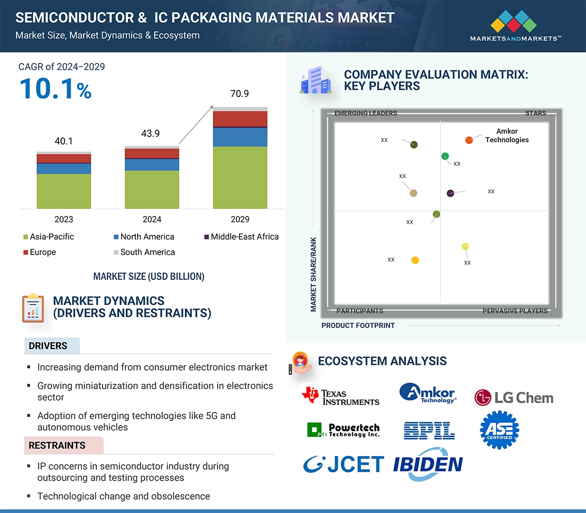
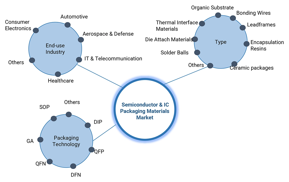
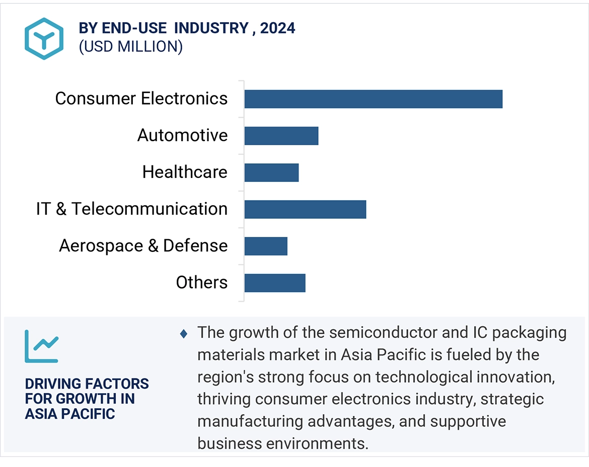
The semiconductor and IC packaging materials market refers to the industry segment focused on producing materials essential for packaging and protecting semiconductor devices and integrated circuits (ICs). These materials include organic substrates, bonding wires, leadframes, encapsulation resins, thermal insulation materials, and solder balls. The market caters to various end-use industries such as consumer electronics, automotive, aerospace, healthcare, and telecommunications. Key factors driving this market include technological advancements, demand for compact and lightweight packaging solutions, rising consumer electronics adoption, and the growth of emerging technologies like AI, IoT, and 5G.

Key Stakeholders

  • Semiconductor & IC packaging materials manufacturers
  • Semiconductor & IC packaging materials traders, distributors, and suppliers
  • End-use industry participants of different segments of the semiconductor & IC packaging materials market
  • Government and research organizations
  • Associations and industrial bodies
  • Research and consulting firms.
  • Research & development (R&D) institutions.

Report Objectives

  • To define, describe, and forecast the size of the semiconductor & IC packaging materials market, in terms of value.
  • To provide detailed information regarding the major factors (drivers, opportunities, restraints, and challenges) influencing the growth of the market
  • To estimate and forecast the market size based on type, packaging technology, end-use industry and region.
  • To forecast the size of the market with respect to major regions, namely, Europe, North America, Asia Pacific, Middle East & Africa, and South America, along with their key countries.
  • To strategically analyze micromarkets1 with respect to individual growth trends, prospects, and their contribution to the overall market.
  • To analyze opportunities in the market for stakeholders and provide a competitive landscape of market leaders.
  • To track and analyze recent developments such as expansions, new product launches, partnerships & agreements, and acquisitions in the market.
  • To strategically profile key market players and comprehensively analyze their core competencies.

Available Customizations

Along with the given market data, MarketsandMarkets offers customizations according to the company’s specific needs. The following customization options are available for the report:

Regional Analysis

  • Further breakdown of a region with respect to a particular country or additional application

Company Information

  • Detailed analysis and profiles of additional market players
Custom Market Research Services

We will customize the research for you, in case the report listed above does not meet with your exact requirements. Our custom research will comprehensively cover the business information you require to help you arrive at strategic and profitable business decisions.

Request Customization
Report Code
CH 2348
Published ON
Mar, 2024
Choose License Type
BUY NOW
  • SHARE
X
Request Customization
Speak to Analyst
Speak to Analyst
OR FACE-TO-FACE MEETING
PERSONALIZE THIS RESEARCH
  • Triangulate with your Own Data
  • Get Data as per your Format and Definition
  • Gain a Deeper Dive on a Specific Application, Geography, Customer or Competitor
  • Any level of Personalization
REQUEST A FREE CUSTOMIZATION
LET US HELP YOU!
  • What are the Known and Unknown Adjacencies Impacting the Semiconductor & IC packaging materials Market
  • What will your New Revenue Sources be?
  • Who will be your Top Customer; what will make them switch?
  • Defend your Market Share or Win Competitors
  • Get a Scorecard for Target Partners
CUSTOMIZED WORKSHOP REQUEST
+1-888-600-6441
  • Call Us
  • +1-888-600-6441 (Corporate office hours)
  • +1-888-600-6441 (US/Can toll free)
  • +44-800-368-9399 (UK office hours)
CONNECT WITH US
ABOUT TRUST ONLINE
©2024 MarketsandMarkets Research Private Ltd. All rights reserved
DMCA.com Protection Status Website Feedback