Thin Wafer Market by Wafer Size (125 mm, 200 mm, and 300 mm), Process (Temporary Bonding & Debonding and Carrier-less/Taiko Process), Technology, Application (MEMS, CIS, Memory, RF Devices, LED, Interposer, Logic) and Geography - Global Forecast to 2027
Updated on : Oct 25, 2024
Rising adoption of MEMS technology in portable health monitoring devices, reducing sizes of electronic devices, growing smartphone and consumer electronics markets and high amount of material saving is expected to fuel the growth of the thin wafer industry.
Thin Wafer Market Size
The global thin wafer market size is projected to grow from USD 11.4 billion in 2022 to reach USD 20.6 billion by 2027; it is expected to grow at a Compound Annual Growth Rate (CAGR) of 12.5% from 2022 to 2027.
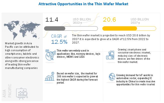
To know about the assumptions considered for the study, Request for Free Sample Report
Thin Wafer Market Dynamics
Driver: Reducing sizes of electronic devices
As electronic devices shrink in size, it creates a requirement for thin ICs. The increasing demand from portable devices for products such as memory, chips, ICs, and RF devices is expected to drive the growth of the thin wafer market. Earlier, the thickness of a mobile phone was around 15–20 mm; however, with technological advancements, it has decreased. Presently, the thickness of a smartphone ranges between 6 mm and 9 mm. Also, other electronic devices such as laptops, tablets, and audio devices have either reduced in thickness or size. The increasing demand for wearables and other portable smart products creates the need for thin wafers, thereby driving market growth.
Restraint: Efficiency maintenance-major issue for thin wafers
Currently, efficiency is the main issue faced by companies in adopting thin wafers. A thin wafer has a low light absorption capacity for long wavelengths, especially if the thickness is below 50 ìm. The distance traveled by the light to be completely absorbed by the wafer is long, in the case long wavelengths. The primary motive behind developing a thin wafer is to ensure that chip manufacturers have the advantage of all the benefits of thin wafers, such as low power consumption, high performance, and smaller die area.
Opportunity: Growing adoption of IoT and AI in automotive sector
The advent of Industry 4.0 and technologies such as IoT and AI in the automotive sector will contribute significantly toward the growth of the thin wafer market. The increased demand for vehicle connectivity will encourage new developments in the industry. Also, with ongoing trends such as touch-free human–machine interfaces revolutionizing the automotive sector, there is a growing significance of connected cars. According to a report published by the IoT Analytics Research in 2022, the number of IoT connections is projected to reach 27.0 billion globally by 2025. Integration of IoT in automotive safety and communication technologies is one of the major reasons for the growth of IoT connections in the future. The introduction of technologies such as advanced driver assistance systems (ADAS), adaptive cruise control, and intelligent parking assistance systems will further drive the market growth. These systems integrate large number of electronic systems which are fabricated using thin wafers, which aid in high performance and smooth functioning of these in-car systems.
Challenge: Volatality and Susceptibility to damage caused by pressure or stress
Thin wafers are volatile and susceptible to damage in the case of pressure or stress. A thin wafer is highly flexible and faces breakage issues even due to little pressure or stress. Dies made from thin wafers can easily break during the internal process of wafer thinning. Companies operating in the thin wafer market are working toward overcoming this challenge by developing support systems to handle a thin wafer through various processes such as wafer bonding and debonding. Also, companies are using a high-quality adhesive in the carrier which handles the thin wafer.
Thin Wafer Ecosystem
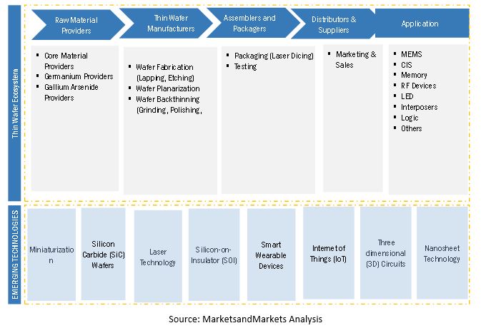
Thin wafer market for CIS applications is expected to grow at a significant CAGR during the forecast period.”
The thin wafer market for CIS application is expected to grow at a significant CAGR during the forecast period. CIS is used in mobile phones and other consumer electronic devices. The miniaturization of these electronic devices generates the need for thick and thin CMOS chips. Hence, to develop thin CIS chips, thin wafers are used during their fabrication. This has led to an increased demand for CIS thereby paving way for the growth of thin wafer market.
Wafer dicing equipment to hold the largest market share of the thin wafer market during the forecast period”
Wafer dicing dominated the thin wafer market in 2021 and is expected to follow the trend during forecast period. An increase in memory capacity and continuous package miniaturization require ultra-thin wafer dicing. In recent years, there has been an increasing adoption of RFID tags and SIP (system in package) for smartphones and other compact electronic devices. This has resulted in the rapid growth of finished semiconductor die with thickness less than or equal to 100 µm. This growing demand has made the processing of thin wafers an essential competence for many integrated device manufacturers. The increasing demand for high-speed dicing combined with superior breakage strength has paved way for an increased demand for the wafer dicing equipment.
Thin wafer market in Asia Pacific estimated to grow at the fastest rate during the forecast period
Asia Pacific plays a pivotal role in the development of the electrical and electronics industry. A few of the leading thin wafer manufacturing companies such as Shin-Etsu Chemical Co., Ltd. (Japan), SUMCO Corporation (Japan), GlobalWafers Co., Ltd. (Taiwan), DISCO Corporation (Japan) are based in Asia Pacific. The high growth of Asia Pacific can be attributed to the surging adoption of high-end consumer electronics, such as wearables and smart home devices in China and Japan. The global semiconductor market is expected to unveil substantial development in the Asia Pacific region due to favorable economic conditions and increasing demand for consumer electronics. As Asia Pacific has low labor cost most of the thin wafers and wafer thinning equipment are manufactured in Asia Pacific and are exported to various regions. The significant growth toward manufacturing and the potential of China, Japan, and Taiwan are largely contributing to this growth trend.
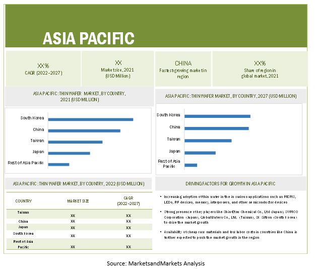
To know about the assumptions considered for the study, download the pdf brochure
Key Market Players
Major thin wafer companies are include Shin-Etsu Chemical Co., Ltd. (Japan), SUMCO Corporation (Japan), GlobalWafers Co., Ltd. (Taiwan), Siltronic (Germany), SK Siltron (South Korea), SUSS MicroTec (Germany), Soitec (France), DISCO Corporation (Japan), 3M (US), and Applied Materials (US). Apart from these, Mechatronic Systemtechnik (Austria), Synova (Switzerland), EV Group (Austria), Wafer Works Corporation (Taiwan), Atecom technology Co., Ltd. (Taiwan), Siltronix Silicon Technologies (France), LDK Solar (China), UniversityWafer, Inc. (US) are among a few emerging companies in the thin wafer market.
Scope of the report
|
Report Metric |
Details |
|
Market size available for years |
2018—2027 |
|
Base year |
2021 |
|
Forecast period |
2022—2027 |
|
Segments covered |
Wafer size, Process, Technnology, Application and Region |
|
Geographic regions covered |
Americas , EMEA and Asia Pacific |
|
Companies covered |
Shin-Etsu Chemical Co., Ltd. (Japan), SUMCO Corporation (Japan), GlobalWafers Co., Ltd. (Taiwan), Siltronic (Germany), SK Siltron (South Korea), SUSS MicroTec (Germany), Soitec (France), DISCO Corporation (Japan), 3M (US), Applied Materials (US), Mechatronic Systemtechnik (Austria), Synova (Switzerland), Brewer Science (US), EV Group (Austria), Wafer Works Corporation (Taiwan), Atecom technology Co., Ltd. (Taiwan), Siltronix Silicon Technologies (France), LDK Solar (China), UniversityWafer, Inc. (US), Wafer World Inc. (US), Silicon Valley Microelectronics (US), Shanghai Simgui Technology Co., Ltd. (China), PV Crystalox Solar PLC (UK) |
This research report categorizes the thin wafer market based on wafer size, process, technnology, application and region
Thin Wafer Market, By Wafer Size:
- 125 mm
- 200 mm
- 300 mm
Thin Wafer Market, By Process:
- Temporary Bonding & Debonding
- Carrier-less/Taiko Process
Thin Wafer Market,
- Grinding
- Polishing
- Dicing
Thin Wafer Market,By Application:
- MEMS
- CIS
- Memory
- RF Devices
- LED
- Interposer
- Logic
- Others
Thin Wafer Market,By Region
- Americas
- EMEA
- Asia Pacific
Recent Developments
- In February 2022, Shin-Etsu Chemical Co., Ltd. (Japan) invested over YEN 80 billion in facility investments for its silicones business, one of its main businesses, with the aim of further expanding and strengthening this business.
- In October 2022, Siltronic (Germany), broke ground for its new manufacturing facility at JTC’s Tampines Wafer Fab Park in Singapore. In partnership with the Singapore Economic Development Board (EDB), Siltronic’s investment of around EUR 2 billion (equivalent to nearly SGD 3 billion) until the end of 2024 will play an important role in meeting the growing semiconductor demand
- In February 2021, Siltronic (Germany) and GlobalWafers Co., Ltd.(Taiwan) agreed on a guarantee for the German Siltronic sites and protection against compulsory redundancies for employees in Germany until the end of 2024. The product portfolios of both companies complement each other in many areas and form a strong basis to benefit from the long-term growth drivers in the wafer industry.
Frequently Asked Questions (FAQ):
What will be the dynamics for the adoption of thin wafer market based on application?
Thin wafer are widely used in memory applications. There is a growing demand for NAND memory in mobile electronics worldwide and the increasing demand for memory due to growing adoption of 5G network. The miniaturization of electronic devices has led to the increase in demand for thin memory chips, which is expected to drive the growth of this segment.
Which wafer size will contribute more to the overall market share by 2027?
The market for 300 mm wafer segment is expected to exhibit highest growth during the forecast period. These wafers offer manufacturers the ability to produce a large number of devices in a single batch. This is one of the reasons companies are developing semiconductor devices that are composed of 300 mm wafers. The market for these wafers is expected to grow at a significant rate due to the growing use of these wafers in LEDs, MEMS, ICs, and many other electronic and semiconductor devices.
How will technological developments such as siliconcarbide technology change the thin wafer landscape in the future?
Silicon Carbide (SiC) is evolving at a rapid space. SiC wafers are largely preferred by semiconductor device manufacturers and fabrication facilities as they offer several advantages over traditional silicon substrates. One of the major advantages of this substrate is its hardness. This substrate is increasingly used for thin wafers to minimize the impact of pressure or stress. Also, SiC has a low coefficient for thermal expansion, which means its shape does not gets altered when subjected to heating or cooling. It can operate on temperatures as high as 1600 °C, which makes it suitable for high-temperature applications. Moreover, this property also helps increase the life of the semiconductor device in which the SiC wafer is installed. Other advantages of SiC wafers include higher power density, reduced switching losses, better heat dissipation, and increased bandwidth capacity. These wafers are increasingly used in the automotive, industrial, and energy industries.
Which region is expected to adopt thin wafers at a fast rate?
Asia Pacific region is expected to adopt thin wafers at the fastest rate. Developing countries such as Taiwan and China are expected to have a high potential for the future growth of the market.
What are the key market dynamics influencing market growth? How will they turn into strengths or weaknesses of companies operating in the market space?
The growth of the thin wafer market can be attributed to factors such rising adoption of MEMS technology in portable health monitoring devices, growing smartphone and consumer electronics markets, reducing sizes of electronic devices, and high amount of material saving.
To speak to our analyst for a discussion on the above findings, click Speak to Analyst

TABLE OF CONTENTS
1 INTRODUCTION (Page No. - 25)
1.1 STUDY OBJECTIVES
1.2 MARKET DEFINITION
1.3 STUDY SCOPE
1.3.1 MARKETS COVERED
1.3.2 INCLUSIONS AND EXCLUSIONS
1.3.3 REGIONAL SCOPE
1.3.4 YEARS CONSIDERED
1.4 CURRENCY
1.5 PACKAGE SIZE
1.6 STAKEHOLDERS
1.7 SUMMARY OF CHANGES
2 RESEARCH METHODOLOGY (Page No. - 29)
2.1 RESEARCH DATA
FIGURE 1 THIN WAFER MARKET: RESEARCH DESIGN
2.1.1 SECONDARY DATA
2.1.1.1 Major secondary sources
2.1.1.2 Key data from secondary sources
2.1.2 PRIMARY DATA
2.1.2.1 Primary interviews with experts
2.1.2.2 Breakdown of primaries
2.1.3 SECONDARY AND PRIMARY RESEARCH
2.1.3.1 Key industry insights
2.2 MARKET SIZE ESTIMATION
FIGURE 2 MARKET SIZE ESTIMATION METHODOLOGY: REVENUE GENERATED BY KEY PLAYERS IN THIN WAFER MARKET
2.2.1 BOTTOM-UP APPROACH
2.2.1.1 Approach to capture market size by bottom-up analysis (demand side)
FIGURE 3 MARKET SIZE ESTIMATION METHODOLOGY: BOTTOM-UP APPROACH
2.2.2 TOP-DOWN APPROACH
2.2.2.1 Approach to capture market size by top-down analysis (supply side)
FIGURE 4 MARKET SIZE ESTIMATION METHODOLOGY: TOP-DOWN APPROACH
2.3 MARKET BREAKDOWN AND DATA TRIANGULATION
FIGURE 5 DATA TRIANGULATION
2.4 RESEARCH ASSUMPTIONS
FIGURE 6 ASSUMPTIONS FOR RESEARCH STUDY
2.5 RISK ASSESSMENT
2.6 LIMITATIONS
3 EXECUTIVE SUMMARY (Page No. - 40)
3.1 GROWTH RATE ASSUMPTIONS/GROWTH FORECAST
FIGURE 7 300 MM WAFER TO ACCOUNT FOR LARGEST MARKET SHARE DURING FORECAST PERIOD
FIGURE 8 THIN WAFER MARKET, BY WAFER SIZE, 2022–2027 (MILLION SQUARE INCHES)
FIGURE 9 MEMORY APPLICATIONS TO DOMINATE THIN WAFER MARKET BY 2027
FIGURE 10 WAFER THINNING EQUIPMENT MARKET FOR LED APPLICATIONS TO GROW AT HIGHEST CAGR BETWEEN 2022 AND 2027
FIGURE 11 ASIA PACIFIC ACCOUNTED FOR LARGEST SHARE OF THIN WAFER MARKET IN 2021
4 PREMIUM INSIGHTS (Page No. - 45)
4.1 ATTRACTIVE OPPORTUNITIES FOR PLAYERS IN THIN WAFER MARKET
FIGURE 12 THIN WAFERS EXPECTED TO WITNESS HIGH ADOPTION RATE DURING FORECAST PERIOD
4.2 WAFER THINNING EQUIPMENT MARKET, BY TECHNOLOGY
FIGURE 13 DICING TECHNOLOGY TO HOLD LARGEST MARKET SHARE DURING FORECAST PERIOD
4.3 THIN WAFER MARKET, BY APPLICATION
FIGURE 14 MARKET FOR LED EXPECTED TO GROW AT HIGHEST CAGR BETWEEN 2022 AND 2027
4.4 WAFER THINNING EQUIPMENT MARKET, BY TECHNOLOGY AND APPLICATION
FIGURE 15 MEMORY AND LOGIC TO BE MOST FAVORABLE APPLICATION AREAS FOR WAFER THINNING EQUIPMENT MARKET IN 2022
4.5 GEOGRAPHICAL ANALYSIS OF THIN WAFER MARKET
FIGURE 16 CHINA TO EXHIBIT HIGHEST CAGR IN THIN WAFER MARKET BETWEEN 2022 AND 2027
5 MARKET OVERVIEW (Page No. - 48)
5.1 INTRODUCTION
5.2 MARKET DYNAMICS
FIGURE 17 THIN WAFER MARKET: DRIVERS, RESTRAINTS, OPPORTUNITIES, AND CHALLENGES
5.2.1 DRIVERS
5.2.1.1 Rising adoption of MEMS technology in portable health monitoring devices
5.2.1.2 Reducing size of electronic devices
5.2.1.3 Growing smartphone and consumer electronics markets
5.2.1.4 High amount of material saving
FIGURE 18 DRIVERS: IMPACT ANALYSIS
5.2.2 RESTRAINTS
5.2.2.1 Efficiency maintenance—major issue for thin wafers
FIGURE 19 RESTRAINTS: IMPACT ANALYSIS
5.2.3 OPPORTUNITIES
5.2.3.1 Expanding IC industry in China
5.2.3.2 Growing adoption of IoT and AI in automotive sector
FIGURE 20 GLOBAL IOT CONNECTIONS FORECAST BY 2025 (BILLION)
5.2.3.3 Rising adoption of portable devices
FIGURE 21 OPPORTUNITIES: IMPACT ANALYSIS
5.2.4 CHALLENGES
5.2.4.1 Volatility and susceptibility to damage caused by pressure or stress
FIGURE 22 CHALLENGES: IMPACT ANALYSIS
5.3 VALUE CHAIN ANALYSIS
FIGURE 23 VALUE CHAIN ANALYSIS: INTEGRATED DEVICE MANUFACTURERS ADD MAJOR VALUE
5.4 ECOSYSTEM/MARKET MAP
TABLE 1 PLAYERS AND THEIR ROLE IN ECOSYSTEM
5.5 TECHNOLOGY ANALYSIS
5.5.1 SILICON CARBIDE (SIC) TECHNOLOGY
TABLE 2 COMPARISON OF BENEFITS OF SIC TECHNOLOGY WITH OTHER TECHNOLOGIES
5.6 CASE STUDY ANALYSIS
5.6.1 STMICROELECTRONICS SELECTS CREE’S SILICON CARBIDE BARE AND EPITAXIAL WAFERS
5.6.2 INFINEON TECHNOLOGIES AND UMC ANNOUNCE MANUFACTURING AGREEMENT
5.6.3 GLOBALWAFERS CO., LTD. AND GLOBALFOUNDRIES ANNOUNCE PARTNERSHIP TO EXPAND SEMICONDUCTOR WAFER SUPPLY
5.6.4 VTT USES OKMETIC’S E-SOI® WAFERS FOR ITS PHOTONICS TECHNOLOGY
5.6.5 SILTERRA MALAYSIA’S NEW MANUFACTURING TECHNOLOGY FOR MEMS AND PHOTONICS DEVICES USES OKMETIC’S C-SOI WAFERS
5.7 REGULATORY LANDSCAPE
5.8 PRICING ANALYSIS
TABLE 3 SELLING PRICE OF THIN WAFER
6 THIN WAFER MARKET, BY PROCESS (Page No. - 62)
6.1 INTRODUCTION
FIGURE 24 TEMPORARY BONDER AND DEBONDER MARKET SIZE
6.2 TEMPORARY BONDING & DEBONDING
6.2.1 MARKET ADHESIVES
6.2.1.1 UV-release adhesives
6.2.1.2 Thermal-release adhesives
6.2.1.3 Solvent-release adhesives
6.3 CARRIER-LESS APPROACH (TAIKO PROCESS)
7 THIN WAFER MARKET, BY WAFER SIZE (Page No. - 65)
7.1 INTRODUCTION
FIGURE 25 300 MM WAFER SEGMENT TO DOMINATE MARKET BETWEEN 2022 AND 2027
TABLE 4 THIN WAFER MARKET, BY WAFER SIZE, 2018–2021 (MILLION SQUARE INCHES)
TABLE 5 THIN WAFER MARKET, BY WAFER SIZE, 2022–2027 (MILLION SQUARE INCHES)
TABLE 6 THIN WAFER MARKET, BY WAFER SIZE, 2018–2021 (USD MILLION)
TABLE 7 THIN WAFER MARKET, BY WAFER SIZE, 2022–2027 (USD MILLION)
7.2 125 MM
7.2.1 ADOPTION OF LARGER DIAMETER WAFERS BY SEMICONDUCTOR MANUFACTURERS TO IMPACT SEGMENT
TABLE 8 125 MM: THIN WAFER MARKET, BY APPLICATION, 2018–2021 (MILLION SQUARE INCHES)
TABLE 9 125 MM: THIN WAFER MARKET, BY APPLICATION, 2022–2027 (MILLION SQUARE INCHES)
TABLE 10 125 MM: THIN WAFER MARKET, BY APPLICATION, 2018–2021 (USD MILLION)
TABLE 11 125 MM: THIN WAFER MARKET, BY APPLICATION, 2022–2027 (USD MILLION)
7.3 200 MM
7.3.1 DEMAND FOR 200 MM WAFERS TO WITNESS STEADY GROWTH DURING FORECAST PERIOD
TABLE 12 200 MM: THIN WAFER MARKET, BY APPLICATION, 2018–2021 (MILLION SQUARE INCHES)
TABLE 13 200 MM: THIN WAFER MARKET, BY APPLICATION, 2022–2027 (MILLION SQUARE INCHES)
TABLE 14 200 MM: THIN WAFER MARKET, BY APPLICATION, 2018–2021 (USD MILLION)
TABLE 15 200 MM: THIN WAFER MARKET, BY APPLICATION, 2022–2027 (USD MILLION)
7.4 300 MM
7.4.1 300 MM WAFER SEGMENT EXPECTED TO WITNESS FASTEST GROWTH DURING FORECAST PERIOD
TABLE 16 300 MM: THIN WAFER MARKET, BY APPLICATION, 2018–2021 (MILLION SQUARE INCHES)
TABLE 17 300 MM: THIN WAFER MARKET, BY APPLICATION, 2022–2027 (MILLION SQUARE INCHES)
TABLE 18 300 MM: THIN WAFER MARKET, BY APPLICATION, 2018–2021 (USD MILLION)
TABLE 19 300 MM: THIN WAFER MARKET, BY APPLICATION, 2022–2027 (USD MILLION)
8 THIN WAFER MARKET, BY APPLICATION (Page No. - 75)
8.1 INTRODUCTION
FIGURE 26 THIN WAFER SHIPMENTS FOR LED APPLICATIONS TO GROW AT HIGHEST RATE BETWEEN 2022 AND 2027
TABLE 20 THIN WAFER MARKET, BY APPLICATION, 2018–2021 (MILLION SQUARE INCHES)
TABLE 21 THIN WAFER MARKET, BY APPLICATION, 2022–2027 (MILLION SQUARE INCHES)
FIGURE 27 MEMORY TO BE LARGEST APPLICATION IN THIN WAFERS MARKET IN 2022
TABLE 22 THIN WAFER MARKET, BY APPLICATION, 2018–2021 (USD MILLION)
TABLE 23 THIN WAFER MARKET, BY APPLICATION, 2022–2027 (USD MILLION)
TABLE 24 WAFER THINNING EQUIPMENT MARKET, BY APPLICATION, 2018–2021 (USD MILLION)
TABLE 25 WAFER THINNING EQUIPMENT MARKET, BY APPLICATION, 2022–2027 (USD MILLION)
8.2 MEMS
8.2.1 GROWTH ATTRIBUTED TO HIGH ADOPTION IN PORTABLE ELECTRONIC DEVICES
TABLE 26 THIN WAFER MARKET FOR MEMS DEVICES, BY WAFER SIZE, 2018–2021 (MILLION SQUARE INCHES)
TABLE 27 THIN WAFER MARKET FOR MEMS DEVICES, BY WAFER SIZE, 2022–2027 (MILLION SQUARE INCHES)
TABLE 28 THIN WAFER MARKET FOR MEMS DEVICES, BY WAFER SIZE, 2018–2021 (USD MILLION)
TABLE 29 THIN WAFER MARKET FOR MEMS DEVICES, BY WAFER SIZE, 2022–2027 (USD MILLION)
TABLE 30 WAFER THINNING EQUIPMENT MARKET FOR MEMS APPLICATIONS, BY REGION, 2018–2021 (USD MILLION)
TABLE 31 WAFER THINNING EQUIPMENT MARKET FOR MEMS APPLICATIONS, BY REGION, 2022–2027 (USD MILLION)
8.3 CIS
8.3.1 INCREASING DEMAND FOR CIS FROM AUTOMOTIVE VERTICAL EXPECTED TO DRIVE DEMAND
TABLE 32 THIN WAFER MARKET FOR CIS APPLICATIONS, BY WAFER SIZE, 2018–2021 (MILLION SQUARE INCHES)
TABLE 33 THIN WAFER MARKET FOR CIS APPLICATIONS, BY WAFER SIZE, 2022–2027 (MILLION SQUARE INCHES)
TABLE 34 THIN WAFER MARKET FOR CIS APPLICATIONS, BY WAFER SIZE, 2018–2021 (USD MILLION)
TABLE 35 THIN WAFER MARKET FOR CIS APPLICATIONS, BY WAFER SIZE, 2022–2027 (USD MILLION)
TABLE 36 WAFER THINNING EQUIPMENT MARKET FOR CIS APPLICATIONS, BY REGION, 2018–2021 (USD MILLION)
TABLE 37 WAFER THINNING EQUIPMENT MARKET FOR CIS APPLICATIONS, BY REGION, 2022–2027 (USD MILLION)
8.4 MEMORY
8.4.1 GROWING ADOPTION OF NAND FLASH MEMORY IN MOBILE ELECTRONICS TO DRIVE DEMAND
TABLE 38 THIN WAFER MARKET FOR MEMORY DEVICES, BY WAFER SIZE, 2018–2021 (MILLION SQUARE INCHES)
TABLE 39 THIN WAFER MARKET FOR MEMORY DEVICES, BY WAFER SIZE, 2022–2027 (MILLION SQUARE INCHES)
TABLE 40 THIN WAFER MARKET FOR MEMORY DEVICES, BY WAFER SIZE, 2018–2021 (USD MILLION)
TABLE 41 THIN WAFER MARKET FOR MEMORY DEVICES, BY WAFER SIZE, 2022–2027 (USD MILLION)
TABLE 42 WAFER THINNING EQUIPMENT MARKET FOR MEMORY APPLICATIONS, BY REGION, 2018–2021 (USD MILLION)
TABLE 43 WAFER THINNING EQUIPMENT MARKET FOR MEMORY APPLICATIONS, BY REGION, 2022–2027 (USD MILLION)
8.5 RF DEVICES
8.5.1 GROWING ADOPTION OF RF DEVICES IN SMARTPHONES TO PROPEL MARKET GROWTH
TABLE 44 THIN WAFER MARKET FOR RF DEVICES, BY WAFER SIZE, 2018–2021 (MILLION SQUARE INCHES)
TABLE 45 THIN WAFER MARKET FOR RF DEVICES, BY WAFER SIZE, 2022–2027 (MILLION SQUARE INCHES)
TABLE 46 THIN WAFER MARKET FOR RF DEVICES, BY WAFER SIZE, 2018–2021 (USD MILLION)
TABLE 47 THIN WAFER MARKET FOR RF DEVICES, BY WAFER SIZE, 2022–2027 (USD MILLION)
TABLE 48 WAFER THINNING EQUIPMENT MARKET FOR RF DEVICES, BY REGION, 2018–2021 (USD MILLION)
TABLE 49 WAFER THINNING EQUIPMENT MARKET FOR RF DEVICES, BY REGION, 2022–2027 (USD MILLION)
8.6 LED
8.6.1 INCREASING DEMAND FOR LED COMPONENTS IN HOMES AND INFRASTRUCTURE TO DRIVE SEGMENT
TABLE 50 THIN WAFER MARKET FOR LED DEVICES, BY WAFER SIZE, 2018–2021 (MILLION SQUARE INCHES)
TABLE 51 THIN WAFER MARKET FOR LED DEVICES, BY WAFER SIZE, 2022–2027 (MILLION SQUARE INCHES)
TABLE 52 THIN WAFER MARKET FOR LED DEVICES, BY WAFER SIZE, 2018–2021 (USD MILLION)
TABLE 53 THIN WAFER MARKET FOR LED DEVICES, BY WAFER SIZE, 2022–2027 (USD MILLION)
TABLE 54 WAFER THINNING EQUIPMENT MARKET FOR LED DEVICES, BY REGION, 2018–2021 (USD MILLION)
TABLE 55 WAFER THINNING EQUIPMENT MARKET FOR LED DEVICES, BY REGION, 2022–2027 (USD MILLION)
8.7 INTERPOSERS
8.7.1 NEED FOR ADVANCED ARCHITECTURE IN MINIATURE ELECTRONIC DEVICES TO DRIVE DEMAND
TABLE 56 THIN WAFER MARKET FOR INTERPOSERS, BY WAFER SIZE, 2018–2021 (MILLION SQUARE INCHES)
TABLE 57 THIN WAFER MARKET FOR INTERPOSERS, BY WAFER SIZE, 2022–2027 (MILLION SQUARE INCHES)
TABLE 58 THIN WAFER MARKET FOR INTERPOSERS, BY WAFER SIZE, 2018–2021 (USD MILLION)
TABLE 59 THIN WAFER MARKET FOR INTERPOSERS, BY WAFER SIZE, 2022–2027 (USD MILLION)
TABLE 60 WAFER THINNING EQUIPMENT MARKET FOR INTERPOSERS, BY REGION, 2018–2021 (USD MILLION)
TABLE 61 WAFER THINNING EQUIPMENT MARKET FOR INTERPOSERS, BY REGION, 2022–2027 (USD MILLION)
8.8 LOGIC
8.8.1 HIGH PENETRATION OF AFFORDABLE CLOUD COMPUTING SOLUTIONS TO DRIVE DEMAND
TABLE 62 THIN WAFER MARKET FOR LOGIC DEVICES, BY WAFER SIZE, 2018–2021 (MILLION SQUARE INCHES)
TABLE 63 THIN WAFER MARKET FOR LOGIC DEVICES, BY WAFER SIZE, 2022–2027 (MILLION SQUARE INCHES)
TABLE 64 THIN WAFER MARKET FOR LOGIC DEVICES, BY WAFER SIZE, 2018–2021 (USD MILLION)
TABLE 65 THIN WAFER MARKET FOR LOGIC DEVICES, BY WAFER SIZE, 2022–2027 (USD MILLION)
TABLE 66 WAFER THINNING EQUIPMENT MARKET LOGIC APPLICATIONS, BY REGION, 2018–2021 (USD MILLION)
TABLE 67 WAFER THINNING EQUIPMENT MARKET FOR LOGIC APPLICATIONS, BY REGION, 2022–2027 (USD MILLION)
8.9 OTHERS
TABLE 68 THIN WAFER MARKET FOR OTHER APPLICATIONS, BY WAFER SIZE, 2018–2021 (MILLION SQUARE INCHES)
TABLE 69 THIN WAFER MARKET FOR OTHER APPLICATIONS, BY WAFER SIZE, 2022–2027 (MILLION SQUARE INCHES)
TABLE 70 THIN WAFER MARKET FOR OTHER APPLICATIONS, BY WAFER SIZE, 2018–2021 (USD MILLION)
TABLE 71 THIN WAFER MARKET FOR OTHER APPLICATIONS, BY WAFER SIZE, 2022–2027 (USD MILLION)
TABLE 72 WAFER THINNING EQUIPMENT MARKET FOR OTHER APPLICATIONS, BY REGION, 2018–2021 (USD MILLION)
TABLE 73 WAFER THINNING EQUIPMENT MARKET FOR OTHER APPLICATIONS, BY REGION, 2022–2027 (USD MILLION)
9 THIN WAFER MARKET, BY TECHNOLOGY (Page No. - 99)
9.1 INTRODUCTION
FIGURE 28 WAFER POLISHING EQUIPMENT MARKET TO GROW AT HIGHEST CAGR BETWEEN 2022 AND 2027
TABLE 74 WAFER THINNING EQUIPMENT MARKET, BY TECHNOLOGY, 2018–2021 (USD MILLION)
TABLE 75 WAFER THINNING EQUIPMENT MARKET, BY TECHNOLOGY, 2022–2027 (USD MILLION)
9.2 WAFER GRINDING
9.2.1 ATTRACTIVE FOR USE IN MINIATURIZATION OF SEMICONDUCTOR DEVICES
TABLE 76 WAFER GRINDING EQUIPMENT MARKET, BY APPLICATION, 2018–2021 (USD MILLION)
TABLE 77 WAFER GRINDING EQUIPMENT MARKET, BY APPLICATION, 2022–2027 (USD MILLION)
TABLE 78 WAFER GRINDING EQUIPMENT MARKET, BY REGION, 2018–2021 (USD MILLION)
TABLE 79 WAFER GRINDING EQUIPMENT MARKET, BY REGION, 2022–2027 (USD MILLION)
9.3 WAFER POLISHING
9.3.1 DEMAND FOR THIN WAFERS WITH SMOOTH SURFACE FOR SEAMLESS INTEGRATION TO DRIVE SEGMENT
TABLE 80 WAFER POLISHING EQUIPMENT MARKET, BY APPLICATION, 2018–2021 (USD MILLION)
TABLE 81 WAFER POLISHING EQUIPMENT MARKET, BY APPLICATION, 2022–2027 (USD MILLION)
TABLE 82 WAFER POLISHING EQUIPMENT MARKET, BY REGION, 2018–2021 (USD MILLION)
TABLE 83 WAFER POLISHING EQUIPMENT MARKET, BY REGION, 2022–2027 (USD MILLION)
9.4 WAFER DICING
9.4.1 WAFER DICING EQUIPMENT TO ACCOUNT FOR LARGEST MARKET SHARE DURING FORECAST PERIOD
TABLE 84 WAFER DICING EQUIPMENT MARKET, BY APPLICATION, 2018–2021 (USD MILLION)
TABLE 85 WAFER DICING EQUIPMENT MARKET, BY APPLICATION, 2022–2027 (USD MILLION)
TABLE 86 WAFER DICING EQUIPMENT MARKET, BY REGION, 2018–2021 (USD MILLION)
TABLE 87 WAFER DICING EQUIPMENT MARKET, BY REGION, 2022–2027 (USD MILLION)
10 THIN WAFER MARKET, BY GEOGRAPHY (Page No. - 108)
10.1 INTRODUCTION
FIGURE 29 THIN WAFER MARKET: GEOGRAPHIC SNAPSHOT, 2022–2027
TABLE 88 THIN WAFER MARKET, BY REGION, 2018–2021 (USD MILLION)
TABLE 89 THIN WAFER MARKET, BY REGION, 2022–2027 (USD MILLION)
TABLE 90 WAFER THINNING EQUIPMENT MARKET, BY REGION, 2018–2021 (USD MILLION)
TABLE 91 WAFER THINNING EQUIPMENT MARKET, BY REGION, 2022–2027 (USD MILLION)
10.2 AMERICAS
FIGURE 30 AMERICAS: GEOGRAPHIC SNAPSHOT
TABLE 92 AMERICAS: THIN WAFER MARKET, BY COUNTRY, 2018–2021 (USD MILLION)
TABLE 93 AMERICAS: THIN WAFER MARKET, BY COUNTRY, 2022–2027 (USD MILLION)
TABLE 94 AMERICAS: WAFER THINNING EQUIPMENT MARKET, BY APPLICATION, 2018–2021 (USD MILLION)
TABLE 95 AMERICAS: WAFER THINNING EQUIPMENT MARKET, BY APPLICATION, 2022–2027 (USD MILLION)
10.2.1 US
10.2.1.1 US to lead thin wafer market in Americas during forecast period
10.2.2 CANADA
10.2.2.1 Government support to promote use of electric vehicles to drive market
10.2.3 REST OF AMERICAS
10.2.3.1 Growing demand for semiconductor devices from consumer electronics and automotive industries to fuel market growth
10.3 EMEA
FIGURE 31 EMEA: GEOGRAPHIC SNAPSHOT
TABLE 96 EMEA: THIN WAFER MARKET, BY COUNTRY, 2018–2021 (USD MILLION)
TABLE 97 EMEA: THIN WAFER MARKET, BY COUNTRY, 2022–2027 (USD MILLION)
TABLE 98 EMEA: WAFER THINNING EQUIPMENT MARKET, BY APPLICATION, 2018–2021 (USD MILLION)
TABLE 99 EMEA: WAFER THINNING EQUIPMENT MARKET, BY APPLICATION, 2022–2027 (USD MILLION)
10.3.1 UK
10.3.1.1 Increase in demand for portable medical devices to drive market
10.3.2 GERMANY
10.3.2.1 Growing adoption of MEMS sensors in automotive industry to drive market
10.3.3 FRANCE
10.3.3.1 Increased EV manufacturing to bolster market growth in France
10.3.4 REST OF EMEA
10.3.4.1 Dearth of thin wafer manufacturers ¯ opportunity for new investments in Rest of EMEA
10.4 ASIA PACIFIC
FIGURE 32 ASIA PACIFIC: GEOGRAPHIC SNAPSHOT
TABLE 100 ASIA PACIFIC: THIN WAFER MARKET, BY COUNTRY, 2018–2021 (USD MILLION)
TABLE 101 ASIA PACIFIC: THIN WAFER MARKET, BY COUNTRY, 2022–2027 (USD MILLION)
TABLE 102 ASIA PACIFIC: WAFER THINNING EQUIPMENT MARKET, BY APPLICATION, 2018–2021 (USD MILLION)
TABLE 103 ASIA PACIFIC: WAFER THINNING EQUIPMENT MARKET, BY APPLICATION, 2022–2027 (USD MILLION)
10.4.1 TAIWAN
10.4.1.1 Presence of several fabrication facilities and IC manufacturing firms to drive market
10.4.2 CHINA
10.4.2.1 China’s focus on achieving 70% IC self-sufficiency by 2025 to drive market
10.4.3 JAPAN
10.4.3.1 Presence of major market players and end-use industries to drive market
10.4.4 SOUTH KOREA
10.4.4.1 South Korea expected to account for largest share of Asia Pacific market during forecast period
10.4.5 REST OF ASIA PACIFIC
10.4.5.1 Growing demand for connected devices to drive market in Rest of Asia Pacific
11 COMPETITIVE LANDSCAPE (Page No. - 125)
11.1 COMPETITIVE LANDSCAPE
TABLE 104 THIN WAFER MARKET: KEY GROWTH STRATEGIES ADOPTED BY COMPANIES FROM 2019 TO 2022
11.2 REVENUE ANALYSIS OF TOP FIVE COMPANIES
FIGURE 33 THREE-YEAR REVENUE ANALYSIS OF TOP FIVE PLAYERS IN THIN WAFER MARKET
11.3 MARKET SHARE ANALYSIS (2021)
TABLE 105 THIN WAFER MARKET: DEGREE OF COMPETITION
11.4 COMPANY EVALUATION MATRIX
11.4.1 STARS
11.4.2 EMERGING LEADERS
11.4.3 PERVASIVE PLAYERS
11.4.4 PARTICIPANTS
FIGURE 34 THIN WAFER MARKET, COMPANY EVALUATION MATRIX, 2021
11.5 START-UP/SME EVALUATION MATRIX
11.5.1 PROGRESSIVE COMPANIES
11.5.2 RESPONSIVE COMPANIES
11.5.3 DYNAMIC COMPANIES
11.5.4 STARTING BLOCKS
FIGURE 35 THIN WAFER MARKET, START-UP/SME EVALUATION QUADRANT, 2021
11.6 THIN WAFER MARKET: COMPANY FOOTPRINT
TABLE 106 COMPANY FOOTPRINT
TABLE 107 COMPANY WAFER SIZE FOOTPRINT
TABLE 108 COMPANY APPLICATION FOOTPRINT
TABLE 109 COMPANY REGIONAL FOOTPRINT
11.7 COMPETITIVE SITUATIONS AND TRENDS
11.7.1 PRODUCT LAUNCHES
TABLE 110 PRODUCT LAUNCHES, 2019–2022
11.7.2 DEALS
TABLE 111 DEALS, 2019–2022
11.7.3 OTHERS
TABLE 112 EXPANSION, 2019–2022
12 COMPANY PROFILES (Page No. - 141)
(Business Overview, Products Offered, Recent Developments, and MnM View (Key strengths/Right to Win, Strategic Choices Made, and Weaknesses and Competitive Threats))*
12.1 INTRODUCTION
12.2 KEY PLAYERS
12.2.1 SK SILTRON
TABLE 113 SK SILTRON: BUSINESS OVERVIEW
FIGURE 36 SK SILTRON: COMPANY SNAPSHOT
12.2.2 SHIN-ETSU CHEMICAL CO., LTD.
TABLE 114 SHIN-ETSU CHEMICAL CO., LTD.: BUSINESS OVERVIEW
FIGURE 37 SHIN-ETSU CHEMICAL CO., LTD.: COMPANY SNAPSHOT
12.2.3 SILTRONIC
TABLE 115 SILTRONIC: BUSINESS OVERVIEW
FIGURE 38 SILTRONIC: COMPANY SNAPSHOT
12.2.4 SUMCO CORPORATION
TABLE 116 SUMCO CORPORATION: BUSINESS OVERVIEW
FIGURE 39 SUMCO CORPORATION: COMPANY SNAPSHOT
12.2.5 GLOBALWAFERS CO., LTD.
TABLE 117 GLOBALWAFERS CO., LTD.: BUSINESS OVERVIEW
FIGURE 40 GLOBALWAFERS CO., LTD.: COMPANY SNAPSHOT
12.2.6 SOITEC
TABLE 118 SOITEC: BUSINESS OVERVIEW
FIGURE 41 SOITEC: COMPANY SNAPSHOT
12.2.7 SUSS MICROTEC
TABLE 119 SUSS MICROTEC: BUSINESS OVERVIEW
FIGURE 42 SUSS MICROTEC: COMPANY SNAPSHOT
12.2.8 DISCO CORPORATION
TABLE 120 DISCO CORPORATION: BUSINESS OVERVIEW
FIGURE 43 DISCO CORPORATION: COMPANY SNAPSHOT
12.2.9 OKMETIC
TABLE 121 OKMETIC: BUSINESS OVERVIEW
12.2.10 3M
TABLE 122 3M: BUSINESS OVERVIEW
FIGURE 44 3M: COMPANY SNAPSHOT
12.2.11 APPLIED MATERIALS
TABLE 123 APPLIED MATERIALS: BUSINESS OVERVIEW
FIGURE 45 APPLIED MATERIALS: COMPANY SNAPSHOT
12.3 OTHER COMPANIES
12.3.1 MECHATRONIC SYSTEMTECHNIK
12.3.2 SYNOVA
12.3.3 EV GROUP
12.3.4 BREWER SCIENCE
12.3.5 WAFER WORKS CORPORATION
12.3.6 ATECOM TECHNOLOGY CO., LTD.
12.3.7 SIL’TRONIX SILICON TECHNOLOGIES
12.3.8 LDK SOLAR
12.3.9 PV CRYSTALOX SOLAR PLC
12.3.10 UNIVERSITYWAFER, INC
12.3.11 SHANGHAI SIMGUI TECHNOLOGY CO., LTD
12.3.12 VIRGINIA SEMICONDUCTOR INC
12.3.13 SILICON VALLEY MICROELECTRONICS
12.3.14 WAFER WORLD INC.
*Details on Business Overview, Products Offered, Recent Developments, and MnM View (Key strengths/Right to Win, Strategic Choices Made, and Weaknesses and Competitive Threats) might not be captured in case of unlisted companies.
13 APPENDIX (Page No. - 191)
13.1 DISCUSSION GUIDE
13.2 KNOWLEDGE STORE: MARKETSANDMARKETS’ SUBSCRIPTION PORTAL
13.3 CUSTOMIZATION OPTIONS
13.4 RELATED REPORTS
13.5 AUTHOR DETAILS
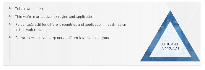
The study involved four major activities in estimating the size for thin wafer market. Exhaustive secondary research was done to collect information on the market, peer market, and parent market. The next step was to validate these findings, assumptions, and sizing with industry experts across value chains through primary research. The bottom-up approach was employed to estimate the overall market size. After that, market breakdown and data triangulation were used to estimate the market size of segments and subsegments.
Secondary Research
In the secondary research process, various sources were used to identify and collect information important for this study. These include annual reports, press releases & investor presentations of companies, white papers, technology journals, and certified publications, articles by recognized authors, directories, and databases.
Secondary research was mainly used to obtain key information about the supply chain of the industry, the total pool of market players, classification of the market according to industry trends to the bottom-most level, regional markets, and key developments from the market and technology-oriented perspectives.
Primary research was also conducted to identify the segmentation types, key players, competitive landscape, and key market dynamics such as drivers, restraints, opportunities, challenges, and industry trends, along with key strategies adopted by players operating in the thin wafer market. Extensive qualitative and quantitative analyses were performed on the complete market engineering process to list key information and insights throughout the report.
Primary Research
Extensive primary research was conducted after obtaining information about the thin wafer market through secondary research. Several primary interviews were conducted with market experts from both the demand and supply sides across 3 major regions, namely the Americas, EMEA, and Asia Pacific. Approximately 80% and 20% of the primary interviews have been conducted with parties from the demand and supply sides, respectively. This primary data was collected through questionnaires, e-mails, and telephonic interviews.
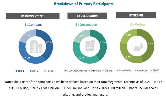
To know about the assumptions considered for the study, download the pdf brochure
Market Size Estimation
In the complete market engineering process, both the top-down and bottom-up approaches were implemented, along with several data triangulation methods, to estimate and validate the size of the thin wafer market and various other dependent submarkets. Key players in the market were identified through secondary research, and their market share in the respective regions was determined through primary and secondary research. This entire research methodology included the study of annual and financial reports of the top players, as well as interviews with experts (such as CEOs, VPs, directors, and marketing executives) for key insights (quantitative and qualitative).
All percentage shares, splits, and breakdowns were determined using secondary sources and verified through primary sources. All the possible parameters that affect the markets covered in this research study were accounted for, viewed in detail, verified through primary research, and analyzed to obtain the final quantitative and qualitative data. This data was consolidated and supplemented with detailed inputs and analysis from MarketsandMarkets and presented in this report.
Thin Wafer Market: Bottom-Up Approach
Data Triangulation
After arriving at the overall market size from the estimation process explained earlier, the overall thin wafer market was split into several segments and subsegments. The data triangulation and market breakdown procedures were employed, wherever applicable to complete the overall market engineering process and arrive at the exact statistics for all segments and subsegments. The data was triangulated by studying various factors and trends from both the demand and supply sides. Along with this, the size of the thin wafer market was validated using top-down and bottom-up approaches.
Report Objectives
- To define, describe, segment, and forecast the global thin wafer market, in terms of value, based on process, wafer size, application, technology, and region
- To forecast the size of the market, by region— Americas, EMEA, and Asia Pacific in terms of value
- To forecast the thin wafer market size, in terms of volume, by process, wafer size, application, technology, and region
- To provide detailed information regarding the drivers, restraints, opportunities, and challenges influencing the growth of the thin wafer market
- To strategically analyze the micromarkets1 with respect to the individual growth trends, prospects, and their contribution to the thin wafer market
- To map the competitive landscape based on company profiles, key player strategies, and key developments
- To provide a detailed overview of the thin wafer market value chain and ecosystem
- To provide information about the key technology trends and patents related to the thin wafer market
- To identify the key players operating in the thin wafer market and comprehensively analyze their market shares and core competencies2
- To analyze opportunities in the market for stakeholders by identifying high-growth segments of the thin wafer market ecosystem
- To benchmark the market players using the proprietary company evaluation matrix framework, which analyzes them on various parameters within the broad categories of market ranking/share and product portfolio
- To analyze competitive developments such as contracts, acquisitions, product launches, collaborations, partnerships, and research and development (R&D) in the thin wafer market
Available Customizations
With the given market data, MarketsandMarkets offers customizations according to the company’s specific needs. The following customization options are available for the report:
Product Analysis
- Product matrix that gives a detailed comparison of the product portfolio of each company
Company Information
- Detailed analysis and profiling of additional market players (up to 7)


 Generating Response ...


Growth opportunities and latent adjacency in Thin Wafer Market
What is the global silica market share and wafer industry market player?