3D IC and 2.5D IC Packaging Market by Packaging Technology (3D Wafer-Level Chip Scale Packaging, 3D TSV and 2.5D), Application (Logic, Memory, MEMS/Sensors, Imaging & Optoelectronics, LED), End User and Region - Global Forecast to 2028
Updated on : October 22, 2024
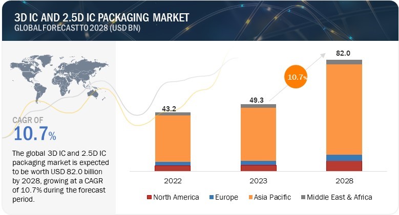
The 3D IC and 2.5D IC packaging market is estimated to be worth USD 49.3 billion in 2022 and is projected to reach USD 82.0 billion by 2028, growing at a CAGR of 10.7% during the forecast period from 2022 to 2028.
Growing adoption of high-end computing, servers, and data centers and miniaturization of IoT Devices are some of the major opportunities that lie ahead for the 3D semiconductor packaging market.
3D IC and 2.5D IC Packaging Market Forecast to 2028
To know about the assumptions considered for the study, Request for Free Sample Report
3D IC and 2.5D IC Packaging Market Dynamics
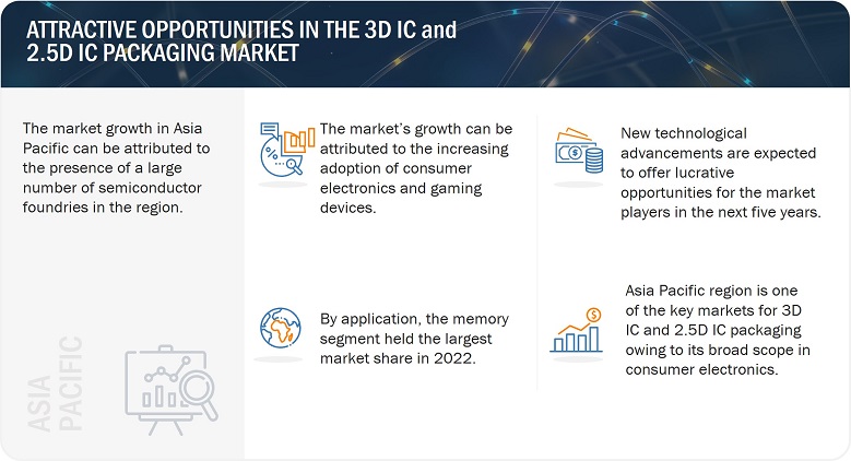
Driver: Growing demand for consumer electronics and gaming devices
With the latest technological advancements, there are many new gadgets coming up in the market, such as e-book readers, gaming devices, tablet computers, 3D smart glass, augmented reality, and virtual reality products which demand high-performance electronic components. 3D IC packaging technology has helped bridge the processor memory performance gap by shortening the critical path and reducing the latency. It also allows scaling to continue efficiently by moving the focus from device-level scaling to circuit- and system-level scaling.
In addition, the advent of 5G technology has fueled the demand for 5G-enabled smartphones. According to Samsung, the demand for smartphones and 5G smartphones is expected to grow at a CAGR of 6% and 37%, respectively, from 2021 to 2025, due to the rising commercialization of 5G technology. Smartphone manufacturers such as Apple Inc., Samsung, Huawei, Vivo, Honor, OPPO, Xiaomi, and OnePlus have commercialized their 5G smartphones worldwide. Thus, the increase in the shipment of 5G smartphones is expected to fuel the demand for 3D IC and 2.5D IC packaging industry during the forecast period.
Restraint: Thermal issues resulting from higher level of integration
3D IC offers highly dense multi-level integration per unit footprint. Though this is attractive for many applications where miniaturization is a concern, it also creates challenges for thermal management; increased integration leads to high on-chip temperature. 3D ICs have several issues that must be resolved, including a larger form factor, the requirement for a larger silicon interposer, and longer design cycles. Overheating is observed during the production of 3D ICs with TSVs. Elevated temperatures result in a drop in threshold voltage and degradation of mobility. The resistance and power dissipation increases as a major part of the component is made up of metal.
Opportunity: Rising number of smart infrastructure and smart city projects
3D IC packaging can play a significant role in the development and implementation of smart city technology. Smart cities rely on a variety of electronic devices, sensors, and systems to collect and analyze data in real time, enabling better decision-making and more efficient resource management. By using 3D IC packaging, these devices and systems can be made smaller and more powerful and energy efficient. This helps reduce the overall cost and size of smart city infrastructure while improving performance and reliability.
Challenge: Reliability challenges with 3D IC packaging
The semiconductor industry business is primarily driven by applications such as data centers/cloud, mobility, and the Internet of Things (IoT). The packaging technique must advance alongside the scaling of integrated circuit (IC) technology in order to fulfill the demands of next-generation information and communication technology (ICT) systems. Package design and development must simultaneously meet cost, performance, form factor, and reliability objectives. In terms of powering the design, the power density is higher for a given footprint than for traditional 2D chips. However, answering reliability issues will be crucial.
3D Semiconductor Packaging Market Insights and Growth Prospects:
The 3D Semiconductor Packaging Market is experiencing significant growth due to the increasing demand for high-performance, space-efficient, and energy-efficient electronic devices. This advanced packaging technology, which involves stacking semiconductor components in multiple layers and connecting them via through-silicon vias (TSVs), offers enhanced performance, reduced device footprint, and improved thermal management. The market is driven by applications in consumer electronics, telecommunications, automotive, and data centers, especially with the rise of IoT, AI, and 5G technologies. As industries seek compact, high-speed solutions, the 3D semiconductor packaging market is expected to expand rapidly, with key players focusing on innovations to offer scalable, cost-effective, and reliable solutions.
3D IC Market Growth Prospects:
The 3D IC Market is poised for rapid growth as demand for high-performance, energy-efficient, and space-saving electronic devices escalates. 3D IC technology enables the stacking of multiple integrated circuits in a single package, connected through vertical interconnects like through-silicon vias (TSVs). This innovation offers significant advantages, including reduced power consumption, faster data processing, and smaller form factors, making it ideal for applications in sectors such as telecommunications, consumer electronics, automotive, and high-performance computing. As industries push for more compact and efficient devices, the 3D IC market is expected to expand, with advancements in packaging technologies driving the adoption of these solutions across a range of applications. Key players in the market are continuously developing new, cost-effective, and scalable 3D IC solutions to meet the growing demands of modern electronics.
3D IC and 2.5D IC Packaging Market Ecosystem
The 3D IC and 2.5D IC packaging technology market is marked by the presence of a few tier-1 companies, such as Samsung Electronics Co. Ltd (South Korea), Taiwan Semiconductor Manufacturing Company Limited (Taiwan), Intel Corporation (US), ASE Technology Holding Co., Ltd. (Taiwan), Amkor Technology (US), Broadcom (US), and many more. These companies have created a competitive ecosystem by investing in research and development activities to launch highly efficient and reliable 3D IC and 2.5D IC packaging solutions.
Consumer electronics to hold largest market share among end users in 3D IC and 2.5D IC packaging market
Consumer electronics, by end user, is expected to hold the largest market share of the 3D IC and 2.5D IC packaging market. Increasing memory requirements in consumer products such as smartphones and tablets are driving the need for various advanced memories such as double-data-rate (DDR) dynamic random-access memory (DRAM), flash memory, and so on to be integrated. The advanced memory architectures are driving the demand for the 3D IC market to offer high-performing, large-capacity, and compact products.
MEMS/Sensors to register highest CAGR in the 3D IC and 2.5D IC packaging market during forecast period
The functional components of MEMS are micro sensors, micro actuators, and microelectronics. The advanced elements of MEMS are accelerometers, gyroscopes, digital compasses, inertial modules, pressure sensors, humidity sensors, microphones, and smart sensors, among others. The key requirement in all these elements and sensors is a miniaturized structure. Therefore, many sensors have started adopting 3D IC and 2.5D IC packages.
3D WLCSP to register highest CAGR in the 3D IC and 2.5D IC packaging market during forecast period
3D WLCSP is one of the most compact package types, with increased functionality and improved thermal performance in printed circuit boards compared to 3D TSV and 2.5D IC. 3D WLCSP has a simplified process design for manufacturing 3D ICs, which uses polymers that can sustain high temperatures, thus addressing the thermal issue, which is the major challenge for this market. 3D WLCSP has gained popularity in space-constrained consumer electronic applications and other portable consumer devices as well as industrial products as it offers cost-effective, small, lightweight, high-performance semiconductor solutions.
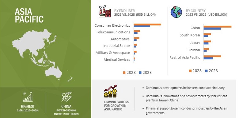
Asia Pacific held to register highest CAGR in the 3D IC and 2.5D IC packaging market during forecast period
The Asia Pacific region is one of the key markets for 3D IC and 2.5D IC packaging owing to its broad scope in various consumer electronics applications, particularly in smartphones and tablets. This is mainly because of the high population density in the region, making it the largest potential market for 3D IC and 2.5D IC packaging among the four major regions.
3D IC and 2.5D IC Packaging Market by Region
To know about the assumptions considered for the study, download the pdf brochure
3D IC and 2.5D IC Packaging Market Key Players
The major players in the 3D IC and 2.5D IC packaging Companies include. The key players such as Samsung (South Korea), Taiwan Semiconductor Manufacturing Company, Ltd. (Taiwan), Intel Corporation (US), ASE Technology Holding Co., Ltd. (Taiwan), Amkor Technology (US), Broadcom (US), Texas Instruments Inc. (US), United Microelectronics Corporation (Taiwan), JCET Group Co., Ltd. (China) and Powertech Technology Inc. (Taiwan). These companies have used both organic and inorganic growth strategies such as product launches, acquisitions, and partnerships to strengthen their position in the 3D semiconductor packaging market.
3D IC and 2.5D IC Packaging Market Report Scope
|
Segment |
Subsegment |
| Estimated Market Size | USD 49.3 Billion |
| Projected Market Size | USD 82.0 Billion |
| Growth Rate | 10.7% |
|
Market size available for years |
2019–2028 |
|
Base year considered |
2022 |
|
Forecast period |
2023–2028 |
|
Forecast units |
Value (USD Million/USD Billion) |
|
Segments covered |
By Packaging Technology, Application, End User, and Region |
|
Geographies covered |
North America, Europe, Asia Pacific, and Rest of World |
|
Companies covered |
The major players in the 3D IC and 2.5D IC packaging market are Samsung (South Korea), Taiwan Semiconductor Manufacturing Company, Ltd. (Taiwan), Intel Corporation (US), ASE Technology Holding Co., Ltd. (Taiwan), Amkor Technology (US), Broadcom (US), Texas Instruments Inc. (US), United Microelectronics Corporation (Taiwan), JCET Group Co., Ltd. (China) and Powertech Technology Inc. (Taiwan) |
3D IC and 2.5D IC Packaging Market Highlights
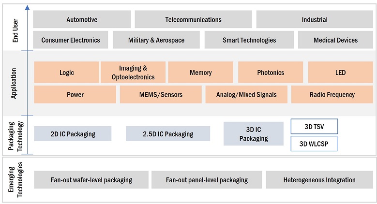
The study segments the 3D IC and 2.5D IC packaging market based on By Packaging Technology, Application, End User, and Region
|
Segment |
Subsegment |
|
By Packaging Technology |
|
|
By Application |
|
|
By End User |
|
|
By Region |
|
Recent Developments in 3D IC and 2.5D IC Packaging Industry
- In February 2023, Amkor Technology (US) has partnered with GlobalFoundries (US), a semiconductor manufacturer. Under the arrangement, foundry chipmaker GlobalFoundries will transfer bump and sort lines for 300 mm wafers from its Dresden wafer fab to Amkor’s facility in Porto, Portugal. This strategic partnership with GlobalFoundries will enhance Amkor's advanced semiconductor packaging supply chain.
- In February 2023, UMC (Taiwan) and Cadence (US) collaborated on 3D-IC Hybrid Bonding Reference Flow. This technology supports the integration across a broad range of technology nodes suitable for edge AI, image processing, and wireless communication applications. Cost-effectiveness and design reliability are the pillars of UMC’s hybrid bonding technologies, and this collaboration with Cadence provides mutual customers with both, helping them reap the benefits of 3D structures while also accelerating the time needed to complete their integrated designs.
- In June 2022, Advanced Semiconductor Engineering, Inc. (ASE), a member of ASE Technology Holding Co., Ltd., launched VIPack, an advanced packaging platform designed to enable vertically integrated package solutions. The platform leverages advanced re-distribution layer (RDL) processes, embedded integration, and 2.5D and 3D technologies to help customers achieve unprecedented innovation when integrating multiple chips within a single package.
Frequently Asked Questions (FAQ):
What is the current size of the global 3D IC and 2.5D IC packaging market?
The 3D IC and 2.5D IC packaging market is estimated to be worth USD 49.3 billion in 2022 and is projected to reach USD 82.0 billion by 2028, at a CAGR of 10.7% during the forecast period.
Who are the winners in the global 3D IC and 2.5D IC packaging market?
Samsung (South Korea), Taiwan Semiconductor Manufacturing Company, Ltd. (Taiwan), Intel Corporation (US), ASE Technology Holding Co., Ltd. (Taiwan), and Amkor Technology (US) are the star companies in the 3D IC and 2.5D IC packaging market.
Which region is expected to hold the highest market share?
Asia Pacific is expected to dominate the 3D IC and 2.5D IC packaging market during forecast period owing to the availability of low-cost labor in China, innovations and advancements by fabrications plants in Taiwan, manufacturing capabilities of Japanese companies, and the establishment of new fabs in China, Taiwan, Japan, and South Korea.
What are the major opportunities related to 3D IC and 2.5D IC packaging market?
Growing adoption of high-end computing, servers, and data centers, miniaturization of IoT Devices and rising number of smart infrastructure and smart city projects are the major opportunities related to 3D IC and 2.5D IC packaging market.
What are the major strategies adopted by market players?
The key players have adopted product launches, acquisitions, and partnerships to strengthen their position in the 3D IC and 2.5D IC packaging market.
To speak to our analyst for a discussion on the above findings, click Speak to Analyst


- 5.1 INTRODUCTION
-
5.2 MARKET DYNAMICSDRIVERS- Increasing need for advanced architecture in electronic products- Rising trend of increased integration density and miniaturization of electronic devices- Growing demand for consumer electronics and gaming devicesRESTRAINTS- Thermal issues resulting from higher level of integration- High unit cost of 3D IC packagesOPPORTUNITIES- Growing adoption of high-end computing, servers, and data centers- Miniaturization of IoT devices- Rising number of smart infrastructure and smart city projectsCHALLENGES- Effective supply chain management- Reliability challenges in 3D IC packaging
-
5.3 SUPPLY CHAIN ANALYSIS
-
5.4 3D IC AND 2.5D IC PACKAGING ECOSYSTEM
- 5.5 REVENUE SHIFT AND NEW REVENUE POCKETS FOR 3D IC AND 2.5D IC PACKAGING MARKET
-
5.6 AVERAGE SELLING PRICE ANALYSISAVERAGE SELLING PRICE OF 3D IC AND 2.5D IC PACKAGING PRODUCTS/SOLUTIONS, BY KEY PLAYERSAVERAGE SELLING PRICE TREND
-
5.7 TECHNOLOGY TRENDSFAN-OUT WAFER-LEVEL PACKAGINGFAN-OUT PANEL-LEVEL PACKAGING
-
5.8 PORTER’S FIVE FORCES ANALYSISTHREAT OF NEW ENTRANTSTHREAT OF SUBSTITUTESBARGAINING POWER OF SUPPLIERSBARGAINING POWER OF BUYERSINTENSITY OF COMPETITIVE RIVALRY
-
5.9 KEY STAKEHOLDERS AND BUYING PROCESS AND/ OR BUYING CRITERIAKEY STAKEHOLDERS IN BUYING PROCESSBUYING CRITERIA
-
5.10 CASE STUDY ANALYSISCLOSED-LOOP MONITORING AND CONTROL BASED ON THERMAL BEHAVIOR REDUCED WAFER REJECTIONSPTS’S DRIE TECHNOLOGY STRENGTHENED IMEC’S SILICON ETCH PLATFORM
-
5.11 TRADE ANALYSISIMPORT SCENARIOEXPORT SCENARIO
-
5.12 PATENT ANALYSIS
- 5.13 KEY CONFERENCES AND EVENTS, 2023–2024
-
5.14 STANDARDS AND REGULATORY LANDSCAPEREGULATORY BODIES, GOVERNMENT AGENCIES, AND OTHER ORGANIZATIONSKEY REGULATIONS AND STANDARDS- North America- Europe- Asia Pacific- Regulations- Standards
- 6.1 INTRODUCTION
-
6.2 3D WAFER-LEVEL CHIP-SCALE PACKAGING (WLCSP)USE OF 3D WLCSP IN CONSUMER ELECTRONICS TO DRIVE MARKET
-
6.3 3D THROUGH-SILICON VIA (TSV)HIGHEST INTERCONNECT DENSITY OFFERED BY 3D TSV TO FUEL DEMAND
-
6.4 2.5DREDUCED COST BENEFIT OFFERED BY 2.5D IC PACKAGING TO DRIVE MARKET
- 7.1 INTRODUCTION
-
7.2 LOGICGROWING PENETRATION OF IOT TO DRIVE MARKET
-
7.3 IMAGING & OPTOELECTRONICSRISING DEMAND FOR SECURITY AND REAL-TIME MONITORING IN AUTOMOBILES TO DRIVE MARKET
-
7.4 MEMORYINCREASED USE OF ARTIFICIAL INTELLIGENCE AND MACHINE LEARNING TO DRIVE MARKET
-
7.5 MEMS/SENSORSADOPTION OF MEMS/SENSORS BY AUTOMOTIVE INDUSTRY TO DRIVE MARKET
-
7.6 LEDSUSE OF LEDS IN FIBER OPTICS TO DRIVE MARKET
- 7.7 OTHERS
- 8.1 INTRODUCTION
-
8.2 CONSUMER ELECTRONICSINCREASING MEMORY REQUIREMENTS IN CONSUMER ELECTRONICS TO FUEL MARKET
-
8.3 INDUSTRIALRISING ADOPTION OF INDUSTRY 4.0 TO DRIVE MARKET
-
8.4 TELECOMMUNICATIONSGROWING USE CASES OF 5G TECHNOLOGY TO FUEL MARKET
-
8.5 AUTOMOTIVEUSE OF IC PACKAGING IN ADAS AND AUTONOMOUS DRIVING TO FUEL MARKET
-
8.6 MILITARY & AEROSPACENEED FOR RELIABLE AND SECURE COMMUNICATION TO FUEL MARKET
-
8.7 MEDICAL DEVICESCAPABILITY TO INCORPORATE MANY SENSORS INTO SINGLE PACKAGE TO FUEL MARKET DEMAND FOR IC PACKAGING
- 9.1 INTRODUCTION
-
9.2 NORTH AMERICAUS- US to lead 3D IC and 2.5D IC packaging market in North AmericaCANADA- Establishment of Canada’s Semiconductor Council to drive regional marketMEXICO- Automotive industry in Mexico to fuel market
-
9.3 EUROPEUK- Increased use of 5G networks to fuel marketGERMANY- Automotive industry to drive marketFRANCE- Highly developed transportation and communication networks to drive marketREST OF EUROPE
-
9.4 ASIA PACIFICCHINA- Increased semiconductor manufacturing to drive marketJAPANTAIWAN- Presence of many key OSAT companies to fuel marketSOUTH KOREA- High manufacturing capacity to drive marketREST OF ASIA PACIFIC
-
9.5 ROWMIDDLE EAST & AFRICASOUTH AMERICA

- 10.1 INTRODUCTION
-
10.2 KEY PLAYER STRATEGIES/RIGHT TO WINPRODUCT PORTFOLIOREGIONAL FOCUSORGANIC/INORGANIC GROWTH STRATEGIES
- 10.3 MARKET SHARE ANALYSIS, 2022
- 10.4 REVENUE ANALYSIS OF TOP PLAYERS IN 3D IC AND 2.5D IC PACKAGING MARKET
-
10.5 KEY COMPANY EVALUATION QUADRANT, 2022STARSPERVASIVE PLAYERSEMERGING LEADERSPARTICIPANTS
-
10.6 COMPETITIVE BENCHMARKINGCOMPANY FOOTPRINT, BY PACKAGING TECHNOLOGYCOMPANY FOOTPRINT, BY REGIONOVERALL COMPANY FOOTPRINT
-
10.7 STARTUP/SMALL AND MEDIUM-SIZED ENTERPRISES (SMES) EVALUATION QUADRANT, 2022COMPETITIVE BENCHMARKING OF KEY STARTUPS/SMES- Company footprint, by packaging technology- Company footprint, by regionPROGRESSIVE COMPANIESRESPONSIVE COMPANIESDYNAMIC COMPANIESSTARTING BLOCKS
-
10.8 COMPETITIVE SITUATION AND TRENDSPRODUCT LAUNCHES AND DEVELOPMENTSDEALS
- 11.1 INTRODUCTION
-
11.2 KEY PLAYERSSAMSUNG- Business overview- Products/Services/Solutions offered- Recent developments- MnM viewTAIWAN SEMICONDUCTOR MANUFACTURING COMPANY LIMITED- Business overview- Products/Services/Solutions offered- Recent developments- MnM viewINTEL CORPORATION- Business overview- Products/Services/Solutions offered- MnM viewASE TECHNOLOGY HOLDING CO., LTD.- Business overview- Products/Services/Solutions offered- Recent developments- MnM viewAMKOR TECHNOLOGY- Business overviews- Products/Services/Solutions offered- Recent developments- MnM viewBROADCOM- Business overview- Products/Services/Solutions offered- Recent developmentsTEXAS INSTRUMENTS INC.- Business overview- Products/Services/Solutions offered- Recent developmentsUNITED MICROELECTRONICS CORPORATION- Business overview- Products/Services/Solutions offered- Recent DevelopmentsJCET GROUP CO., LTD.- Business overview- Products/Services/Solutions offered- Recent developmentsPOWERTECH TECHNOLOGY INC.- Business overview- Products/Services/Solutions offered
-
11.3 OTHER PLAYERSCADENCE DESIGN SYSTEMS, INC.SILICONWARE PRECISION INDUSTRIES CO., LTD.ADVANCED MICRO DEVICES, INC.TEZZARONTELEDYNE TECHNOLOGIES INCORPORATEDFUJITSUXPERI INC.MONOLITHIC 3D INC.DECA TECHNOLOGIES3MGLOBALFOUNDRIES INC.NHANCED SEMICONDUCTORSMOLDEX3DCEREBRASAYAR LABS, INC.
- 12.1 DISCUSSION GUIDE
- 12.2 KNOWLEDGESTORE: MARKETSANDMARKETS’ SUBSCRIPTION PORTAL
- 12.3 CUSTOMIZATION OPTIONS
- 12.4 RELATED REPORTS
- 12.5 AUTHOR DETAILS
- TABLE 1 ASSUMPTIONS FOR RESEARCH STUDY
- TABLE 2 AVERAGE SELLING PRICE OF 12-INCH EQUIVALENT WAFERS, 2022 (THOUSAND UNITS)
- TABLE 3 AVERAGE SELLING PRICE: 3D IC AND 2.5D IC PACKAGING MARKET, 12-INCH EQUIVALENT WAFERS, (USD/THOUSAND UNITS)
- TABLE 4 MARKET: PORTER’S FIVE FORCES ANALYSIS
- TABLE 5 INFLUENCE OF STAKEHOLDERS ON BUYING PROCESS FOR TOP 3 VERTICALS (%)
- TABLE 6 KEY BUYING CRITERIA FOR TOP THREE VERTICALS
- TABLE 7 IMPORT DATA, BY COUNTRY, 2018–2022 (USD MILLION)
- TABLE 8 EXPORT DATA, BY COUNTRY, 2018–2022 (USD MILLION)
- TABLE 9 NOTABLE PATENTS RELATED TO MARKET, 2020–2023
- TABLE 10 NUMBER OF PATENTS REGISTERED RELATED TO MARKET IN LAST 10 YEARS
- TABLE 11 3D IC AND 2.5D IC PACKAGING MARKET: KEY CONFERENCES AND EVENTS
- TABLE 12 NORTH AMERICA: REGULATORY BODIES, GOVERNMENT AGENCIES, AND OTHER ORGANIZATIONS
- TABLE 13 EUROPE: REGULATORY BODIES, GOVERNMENT AGENCIES, AND OTHER ORGANIZATIONS
- TABLE 14 ASIA PACIFIC: REGULATORY BODIES, GOVERNMENT AGENCIES, AND OTHER ORGANIZATIONS
- TABLE 15 COMPARISON BETWEEN 2.5D AND 3D IC TECHNOLOGIES
- TABLE 16 MARKET, BY PACKAGING TECHNOLOGY, 2019–2022 (USD MILLION)
- TABLE 17 3D IC AND 2.5D IC PACKAGING MARKET, BY PACKAGING TECHNOLOGY, 2023–2028 (USD MILLION)
- TABLE 18 3D WLCSP: MARKET, BY END USER, 2019–2022 (USD MILLION)
- TABLE 19 3D WLCSP: 3D PACKAGING MARKET, BY END USER, 2023–2028 (USD MILLION)
- TABLE 20 3D TSV: MARKET, BY END USER, 2019–2022 (USD MILLION)
- TABLE 21 3D TSV: MARKET, BY END USER, 2023–2028 (USD MILLION)
- TABLE 22 2.5D: MARKET, BY END USER, 2019–2022 (USD MILLION)
- TABLE 23 2.5D WLCSP: MARKET, BY END USER, 2023–2028 (USD MILLION)
- TABLE 24 3D IC AND 2.5D IC PACKAGING MARKET, BY APPLICATION, 2019–2022 (USD MILLION)
- TABLE 25 MARKET, BY APPLICATION, 2023–2028 (USD MILLION)
- TABLE 26 LOGIC: MARKET, BY END USER, 2019–2022 (USD MILLION)
- TABLE 27 LOGIC: MARKET, BY END USER, 2023–2028 (USD MILLION)
- TABLE 28 IMAGING & OPTOELECTRONICS: MARKET, BY END USER, 2019–2022 (USD MILLION)
- TABLE 29 IMAGING & OPTOELECTRONICS: MARKET, BY END USER, 2023–2028 (USD MILLION)
- TABLE 30 MEMORY: 3D IC MARKET, BY END USER, 2019–2022 (USD MILLION)
- TABLE 31 MEMORY: MARKET, BY END USER, 2023–2028 (USD MILLION)
- TABLE 32 MEMS/SENSORS: MARKET, BY END USER, 2019–2022 (USD MILLION)
- TABLE 33 MEMS/SENSORS: MARKET, BY END USER, 2023–2028 (USD MILLION)
- TABLE 34 LEDS: 3D IC AND 2.5D IC PACKAGING MARKET, BY END USER, 2019–2022 (USD MILLION)
- TABLE 35 LEDS: 3D SEMICONDUCTOR PACKAGING MARKET, BY END USER, 2023–2028 (USD MILLION)
- TABLE 36 OTHERS: MARKET, BY END USER, 2019–2022 (USD MILLION)
- TABLE 37 OTHERS: MARKET, BY END USER, 2023–2028 (USD MILLION)
- TABLE 38 MARKET, BY END USER, 2019–2022 (USD MILLION)
- TABLE 39 3D IC AND 2.5D IC PACKAGING MARKET, BY END USER, 2023–2028 (USD MILLION)
- TABLE 40 CONSUMER ELECTRONICS: 3D SEMICONDUCTOR PACKAGING MARKET, BY APPLICATION, 2019–2022 (USD MILLION)
- TABLE 41 CONSUMER ELECTRONICS: MARKET, BY APPLICATION, 2023–2028 (USD MILLION)
- TABLE 42 CONSUMER ELECTRONICS: MARKET, BY PACKAGING TECHNOLOGY, 2019–2022 (USD MILLION)
- TABLE 43 CONSUMER ELECTRONICS: 3D PACKAGING MARKET, BY PACKAGING TECHNOLOGY, 2023–2028 (USD MILLION)
- TABLE 44 INDUSTRIAL: MARKET, BY APPLICATION, 2019–2022 (USD MILLION)
- TABLE 45 INDUSTRIAL: MARKET, BY APPLICATION, 2023–2028 (USD MILLION)
- TABLE 46 INDUSTRIAL: MARKET, BY PACKAGING TECHNOLOGY, 2019–2022 (USD MILLION)
- TABLE 47 INDUSTRIAL: MARKET, BY PACKAGING TECHNOLOGY, 2023–2028 (USD MILLION)
- TABLE 48 TELECOMMUNICATIONS: 3D IC AND 2.5D IC PACKAGING MARKET, BY APPLICATION, 2019–2022 (USD MILLION)
- TABLE 49 TELECOMMUNICATIONS: 3D SEMICONDUCTOR PACKAGING MARKET, BY APPLICATION, 2023–2028 (USD MILLION)
- TABLE 50 TELECOMMUNICATIONS: MARKET, BY PACKAGING TECHNOLOGY, 2019–2022 (USD MILLION)
- TABLE 51 TELECOMMUNICATIONS: MARKET, BY PACKAGING TECHNOLOGY, 2023–2028 (USD MILLION)
- TABLE 52 AUTOMOTIVE: MARKET, BY APPLICATION, 2019–2022 (USD MILLION)
- TABLE 53 AUTOMOTIVE: MARKET, BY APPLICATION, 2023–2028 (USD MILLION)
- TABLE 54 AUTOMOTIVE: MARKET, BY PACKAGING TECHNOLOGY, 2019–2022 (USD MILLION)
- TABLE 55 AUTOMOTIVE: MARKET, BY PACKAGING TECHNOLOGY, 2023–2028 (USD MILLION)
- TABLE 56 MILITARY & AEROSPACE: 3D IC AND 2.5D IC PACKAGING MARKET, BY APPLICATION, 2019–2022 (USD MILLION)
- TABLE 57 MILITARY & AEROSPACE: MARKET, BY APPLICATION, 2023–2028 (USD MILLION)
- TABLE 58 MILITARY & AEROSPACE: MARKET, BY PACKAGING TECHNOLOGY, 2019–2022 (USD MILLION)
- TABLE 59 MILITARY & AEROSPACE: 3D PACKAGING MARKET, BY PACKAGING TECHNOLOGY, 2023–2028 (USD MILLION)
- TABLE 60 MEDICAL DEVICES: 3D SEMICONDUCTOR PACKAGING MARKET, BY APPLICATION, 2019–2022 (USD MILLION)
- TABLE 61 MEDICAL DEVICES: MARKET, BY APPLICATION, 2023–2028 (USD MILLION)
- TABLE 62 MEDICAL DEVICES: MARKET, BY PACKAGING TECHNOLOGY, 2019–2022 (USD MILLION)
- TABLE 63 MEDICAL DEVICES: MARKET, BY PACKAGING TECHNOLOGY, 2023–2028 (USD MILLION)
- TABLE 64 3D IC AND 2.5D IC PACKAGING MARKET, BY REGION, 2019–2022 (USD MILLION)
- TABLE 65 MARKET, BY REGION, 2023–2028 (USD MILLION)
- TABLE 66 NORTH AMERICA: 3D SEMICONDUCTOR PACKAGING MARKET, BY COUNTRY, 2019–2022 (USD MILLION)
- TABLE 67 NORTH AMERICA: MARKET, BY COUNTRY, 2023–2028 (USD MILLION)
- TABLE 68 NORTH AMERICA: MARKET, BY END USER, 2019–2022 (USD MILLION)
- TABLE 69 NORTH AMERICA: MARKET, BY END USER, 2023–2028 (USD MILLION)
- TABLE 70 US: MARKET, BY END USER, 2019–2022 (USD MILLION)
- TABLE 71 US: MARKET, BY END USER, 2023–2028 (USD MILLION)
- TABLE 72 CANADA: 3D IC AND 2.5D IC PACKAGING MARKET, BY END USER, 2019–2022 (USD MILLION)
- TABLE 73 CANADA: MARKET, BY END USER, 2023–2028 (USD MILLION)
- TABLE 74 MEXICO: MARKET, BY END USER, 2019–2022 (USD MILLION)
- TABLE 75 MEXICO: MARKET, BY END USER, 2023–2028 (USD MILLION)
- TABLE 76 EUROPE: MARKET, BY COUNTRY, 2019–2022 (USD MILLION)
- TABLE 77 EUROPE: MARKET, BY COUNTRY, 2023–2028 (USD MILLION)
- TABLE 78 EUROPE: MARKET, BY END USER, 2019–2022 (USD MILLION)
- TABLE 79 EUROPE: MARKET, BY END USER, 2023–2028 (USD MILLION)
- TABLE 80 UK: 3D IC AND 2.5D IC PACKAGING MARKET, BY END USER, 2019–2022 (USD MILLION)
- TABLE 81 UK: MARKET, BY END USER, 2023–2028 (USD MILLION)
- TABLE 82 GERMANY: MARKET, BY END USER, 2019–2022 (USD MILLION)
- TABLE 83 GERMANY: MARKET, BY END USER, 2023–2028 (USD MILLION)
- TABLE 84 FRANCE: MARKET, BY END USER, 2019–2022 (USD MILLION)
- TABLE 85 FRANCE: MARKET, BY END USER, 2023–2028 (USD MILLION)
- TABLE 86 REST OF EUROPE: MARKET, BY END USER, 2019–2022 (USD MILLION)
- TABLE 87 REST OF EUROPE: MARKET, BY END USER, 2023–2028 (USD MILLION)
- TABLE 88 ASIA PACIFIC: 3D IC AND 2.5D IC PACKAGING MARKET, BY COUNTRY, 2019–2022 (USD MILLION)
- TABLE 89 ASIA PACIFIC: MARKET, BY COUNTRY, 2023–2028 (USD MILLION)
- TABLE 90 ASIA PACIFIC: MARKET, BY END USER, 2019–2022 (USD MILLION)
- TABLE 91 ASIA PACIFIC: 3D IC MARKET, BY END USER, 2023–2028 (USD MILLION)
- TABLE 92 CHINA: MARKET, BY END USER, 2019–2022 (USD MILLION)
- TABLE 93 CHINA: MARKET, BY END USER, 2023–2028 (USD MILLION)
- TABLE 94 JAPAN: MARKET, BY END USER, 2019–2022 (USD MILLION)
- TABLE 95 JAPAN: 3D IC MARKET, BY END USER, 2023–2028 (USD MILLION)
- TABLE 96 TAIWAN: MARKET, BY END USER, 2019–2022 (USD MILLION)
- TABLE 97 TAIWAN: MARKET, BY END USER, 2023–2028 (USD MILLION)
- TABLE 98 SOUTH KOREA: 3D IC AND 2.5D IC PACKAGING MARKET, BY END USER, 2019–2022 (USD MILLION)
- TABLE 99 SOUTH KOREA: MARKET, BY END USER, 2023–2028 (USD MILLION)
- TABLE 100 REST OF ASIA PACIFIC: MARKET, BY END USER, 2019–2022 (USD MILLION)
- TABLE 101 REST OF ASIA PACIFIC: MARKET, BY END USER, 2023–2028 (USD MILLION)
- TABLE 102 ROW: 3D IC MARKET, BY REGION, 2019–2022 (USD MILLION)
- TABLE 103 ROW: MARKET, BY REGION, 2023–2028 (USD MILLION)
- TABLE 104 ROW: MARKET, BY END USER, 2019–2022 (USD MILLION)
- TABLE 105 ROW: 3D IC AND 2.5D IC PACKAGING MARKET, BY END USER, 2023–2028 (USD MILLION)
- TABLE 106 MIDDLE EAST & AFRICA: MARKET, BY END USER, 2019–2022 (USD MILLION)
- TABLE 107 MIDDLE EAST & AFRICA: MARKET, BY END USER, 2023–2028 (USD MILLION)
- TABLE 108 SOUTH AMERICA: MARKET, BY END USER, 2019–2022 (USD MILLION)
- TABLE 109 SOUTH AMERICA: MARKET, BY END USER, 2023–2028 (USD MILLION)
- TABLE 110 OVERVIEW OF STRATEGIES DEPLOYED BY KEY PLAYERS IN 3D IC AND 2.5D IC PACKAGING MARKET
- TABLE 111 3D IC MARKET SHARE ANALYSIS (2022)
- TABLE 112 MARKET: LIST OF KEY STARTUPS/SMES
- TABLE 113 MARKET: PRODUCT LAUNCHES/DEVELOPMENTS, 2019–2023
- TABLE 114 3D IC AND 2.5D IC PACKAGING MARKET: DEALS, 2019–2023
- TABLE 115 SAMSUNG: BUSINESS OVERVIEW
- TABLE 116 TAIWAN SEMICONDUCTOR MANUFACTURING COMPANY LIMITED: BUSINESS OVERVIEW
- TABLE 117 INTEL CORPORATION: BUSINESS OVERVIEW
- TABLE 118 ASE TECHNOLOGY HOLDING CO., LTD: BUSINESS OVERVIEW
- TABLE 119 AMKOR TECHNOLOGY: BUSINESS OVERVIEW
- TABLE 120 BROADCOM: BUSINESS OVERVIEW
- TABLE 121 TEXAS INSTRUMENTS INC.: BUSINESS OVERVIEW
- TABLE 122 UNITED MICROELECTRONICS CORPORATION: BUSINESS OVERVIEW
- TABLE 123 JCET GROUP CO., LTD.: BUSINESS OVERVIEW
- TABLE 124 POWERTECH TECHNOLOGY INC.: BUSINESS OVERVIEW
- FIGURE 1 3D IC AND 2.5D IC PACKAGING MARKET: SEGMENTATION
- FIGURE 2 MARKET: RESEARCH DESIGN
- FIGURE 3 PROCESS FLOW OF MARKET SIZE ESTIMATION
- FIGURE 4 MARKET SIZE ESTIMATION METHODOLOGY: BOTTOM-UP APPROACH
- FIGURE 5 MARKET SIZE ESTIMATION METHODOLOGY: TOP-DOWN APPROACH
- FIGURE 6 MARKET SIZE ESTIMATION METHODOLOGY: TOP-DOWN APPROACH (SUPPLY SIDE)—REVENUE GENERATED FROM 3D IC AND 2.5D IC PACKAGING SOLUTIONS AND SERVICES
- FIGURE 7 DATA TRIANGULATION
- FIGURE 8 RECESSION IMPACT: GDP GROWTH PROJECTION UNTIL 2023 FOR MAJOR ECONOMIES
- FIGURE 9 RECESSION IMPACT ON 3D IC AND 2.5D IC PACKAGING MARKET, 2019–2028 (USD MILLION)
- FIGURE 10 CONSUMER ELECTRONICS TO HOLD LARGEST MARKET SHARE AMONG END USERS IN MARKET
- FIGURE 11 MEMORY TO HOLD LARGEST MARKET SHARE AMONG APPLICATIONS IN MARKET
- FIGURE 12 2.5D PACKAGING TECHNOLOGY TO CONTINUE TO HOLD LARGEST MARKET SHARE IN MARKET DURING FORECAST PERIOD
- FIGURE 13 3D IC AND 2.5D IC PACKAGING MARKET IN ASIA PACIFIC TO EXHIBIT FASTEST GROWTH DURING FORECAST PERIOD
- FIGURE 14 INCREASED ADOPTION OF CONSUMER ELECTRONICS AND GAMING DEVICES TO BOOST MARKET GROWTH
- FIGURE 15 MILITARY & AEROSPACE TO REGISTER HIGHEST CAGR FROM 2023 TO 2028
- FIGURE 16 2.5D TO HOLD LARGEST SHARE OF MARKET IN 2028
- FIGURE 17 MEMORY TO HOLD LARGEST SHARE OF MARKET IN 2028
- FIGURE 18 CONSUMER ELECTRONICS VERTICAL AND CHINA WERE LARGEST SHAREHOLDERS IN ASIA PACIFIC MARKET IN 2022
- FIGURE 19 MARKET IN MEXICO EXPECTED TO GROW AT FASTEST RATE DURING FORECAST PERIOD
- FIGURE 20 DRIVERS, RESTRAINTS, OPPORTUNITIES, AND CHALLENGES: 3D IC AND 2.5D IC PACKAGING MARKET
- FIGURE 21 ANALYSIS OF IMPACT OF DRIVERS ON MARKET
- FIGURE 22 NUMBER OF SMARTPHONE AND MOBILE PHONE USERS GLOBALLY, 2020–2025 (BILLION)
- FIGURE 23 ANALYSIS OF IMPACT OF RESTRAINTS ON MARKET
- FIGURE 24 ANALYSIS OF IMPACT OF OPPORTUNITIES ON MARKET
- FIGURE 25 ANALYSIS OF IMPACT OF CHALLENGES ON MARKET
- FIGURE 26 SUPPLY CHAIN ANALYSIS: 3D IC AND 2.5D IC PACKAGING MARKET
- FIGURE 27 3D IC AND 2.5D IC PACKAGING ECOSYSTEM
- FIGURE 28 REVENUE SHIFT IN MARKET
- FIGURE 29 AVERAGE SELLING PRICE OF 3D IC AND 2.5D IC PACKAGING PRODUCTS/SOLUTIONS, BY KEY PLAYERS
- FIGURE 30 AVERAGE SELLING PRICE: MARKET, BY WAFER (USD/THOUSAND UNITS)
- FIGURE 31 PORTER’S FIVE FORCES ANALYSIS
- FIGURE 32 INFLUENCE OF STAKEHOLDERS ON BUYING PROCESS FOR TOP 3 END USERS
- FIGURE 33 KEY BUYING CRITERIA FOR TOP THREE VERTICALS
- FIGURE 34 NUMBER OF PATENTS GRANTED PER YEAR, 2013–2022
- FIGURE 35 TOP 10 COMPANIES WITH HIGHEST NUMBER OF PATENT APPLICATIONS IN LAST 10 YEARS
- FIGURE 36 3D IC AND 2.5D IC PACKAGING MARKET, BY PACKAGING TECHNOLOGY
- FIGURE 37 MARKET FOR 3D WLCSP TO GROW AT HIGHEST CAGR DURING FORECAST PERIOD
- FIGURE 38 MARKET, BY APPLICATION
- FIGURE 39 MEMS/SENSORS TO RECORD HIGHEST CAGR DURING FORECAST PERIOD
- FIGURE 40 MILITARY & AEROSPACE MARKET TO GROW AT HIGHEST CAGR FROM 2023 TO 2028
- FIGURE 41 MARKET, BY END USER
- FIGURE 42 MILITARY & AEROSPACE MARKET TO GROW AT HIGHEST CAGR DURING FORECAST PERIOD
- FIGURE 43 ASIA PACIFIC TO WITNESS HIGHEST CAGR IN MARKET DURING FORECAST PERIOD
- FIGURE 44 NORTH AMERICA: MARKET SNAPSHOT
- FIGURE 45 CONSUMER ELECTRONICS TO HOLD LARGEST MARKET SHARE IN NORTH AMERICAN 3D IC AND 2.5D IC PACKAGING MARKET DURING FORECAST PERIOD
- FIGURE 46 EUROPE: MARKET SNAPSHOT
- FIGURE 47 ASIA PACIFIC: MARKET SNAPSHOT
- FIGURE 48 MILITARY & AEROSPACE SEGMENT IN ASIA PACIFIC MARKET TO RECORD HIGHEST CAGR DURING FORECAST PERIOD
- FIGURE 49 FIVE-YEAR REVENUE ANALYSIS OF TOP PLAYERS IN MARKET
- FIGURE 50 3D IC AND 2.5D IC PACKAGING MARKET (GLOBAL): KEY COMPANY EVALUATION QUADRANT, 2022
- FIGURE 51 MARKET (GLOBAL): STARTUPS/SMES EVALUATION QUADRANT, 2022
- FIGURE 52 SAMSUNG: COMPANY SNAPSHOT
- FIGURE 53 TAIWAN SEMICONDUCTOR MANUFACTURING COMPANY LTD.: COMPANY SNAPSHOT
- FIGURE 54 INTEL CORPORATION: COMPANY SNAPSHOT
- FIGURE 55 ASE TECHNOLOGY HOLDING CO., LTD.: COMPANY SNAPSHOT
- FIGURE 56 AMKOR TECHNOLOGY: COMPANY SNAPSHOT
- FIGURE 57 BROADCOM: COMPANY SNAPSHOT
- FIGURE 58 TEXAS INSTRUMENTS INC.: COMPANY SNAPSHOT
- FIGURE 59 UNITED MICROELECTRONICS CORPORATION: COMPANY SNAPSHOT
- FIGURE 60 JCET GROUP CO., LTD.: COMPANY SNAPSHOT
- FIGURE 61 POWERTECH TECHNOLOGY INC.: COMPANY SNAPSHOT
The research study involved 4 major activities in estimating the size of the 3D IC and 2.5D IC packaging market. Exhaustive secondary research has been done to collect important information about the market and peer markets. The validation of these findings, assumptions, and sizing with the help of primary research with industry experts across the value chain has been the next step. Both top-down and bottom-up approaches have been used to estimate the market size. Post which the market breakdown and data triangulation have been adopted to estimate the market sizes of segments and sub-segments.
Secondary Research
In the secondary research process, various secondary sources were referred to for identifying and collecting information required for this study. The secondary sources include annual reports, press releases, and investor presentations of companies, white papers, and articles from recognized authors. Secondary research was mainly done to obtain key information about the market’s value chain, the pool of key market players, market segmentation according to industry trends, and regional outlook and developments from both market and technology perspectives.
Primary Research
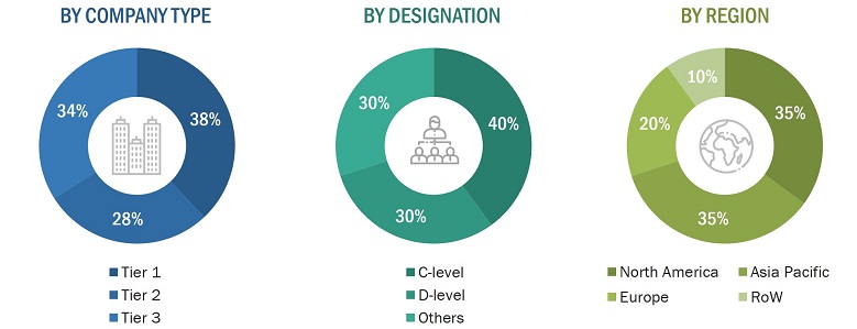
In the primary research, various primary sources from both supply and demand sides were interviewed to obtain qualitative and quantitative insights required for this report. Primary sources from the supply side include experts such as CEOs, vice presidents, marketing directors, equipment manufacturers, technology and innovation directors, end users, and related executives from multiple key companies and organizations operating in the 3D IC and 2.5D IC market ecosystem.
To know about the assumptions considered for the study, download the pdf brochure
Market Size Estimation
In the complete market engineering process, both top-down and bottom-up approaches were used along with several data triangulation methods to estimate and forecast the overall market segments and subsegments listed in this report.
Estimating market size by bottom-up approach (demand side)
- Identifying the entities in the semiconductor value chain influencing the entire 3D IC and 2.5D IC packaging industry, along with the related software and service providers
- Analyzing each type of entity along with related major companies identifying service providers for the implementation of products and services
- Estimating the market for these 3D IC and 2.5D IC end users
- Understanding the demand generated by the semiconductor industry-related companies
- Tracking ongoing and upcoming implementation of 3D IC and 2.5D IC packaging developments by various companies and forecasting the market based on these developments and other critical parameters
- Arriving at the market size by analyzing 3D IC and 2.5D IC packaging companies based on their countries, and then combining it to get the market estimate by region
- Verifying estimates and crosschecking them by a discussion with key opinion leaders, which include CXOs, directors, and operation managers
- Studying various paid and unpaid sources of information, such as annual reports, press releases, white papers, databases, and so on
Market Size Estimation Methodology-Bottom-up Approach

Data Triangulation
After arriving at the overall market size from the market size estimation process explained in the previous section, the total market was split into several segments and subsegments. Data triangulation procedure was employed, wherever applicable, to complete the overall market engineering process and arrive at the exact statistics for all segments and subsegments. The data was triangulated by studying various factors and trends from the demand and supply sides, and the market size was validated using top-down and bottom-up approaches.
Market Definition
A three-dimensional integrated circuit (3D IC) is a package with multiple layers of silicon wafers stalked together, along with electronic components using through-silicon vias (TSVs), while a 2.5-dimensional integrated circuit (2.5D IC) is a package with active electronic components (for example, a die or a chip) stacked on an interposer through conductive bumps or TSVs.
Stakeholders
- Suppliers of Raw Materials and Manufacturing Equipment
- Providers and Manufacturers of Components
- Providers of Software Solutions
- Manufacturers and Providers of Semiconductor Devices
- Original Equipment Manufacturers (OEMs)
- ODM and OEM Technology Solution Providers
- Suppliers and Distributors of Semiconductor Manufacturing Devices
- System Integrators
- Middleware Providers
- Assembly, Testing, and Packaging Vendors
- Market Research and Consulting Firms
- Associations, Organizations, Forums, and Alliances Related to the Semiconductor Packaging
- Technology Investors
- Governments, Regulatory Bodies, and Financial Institutions
- Venture Capitalists, Private Equity Firms, and Startups
- End Users
The main objectives of this study are as follows:
- To define, describe, and forecast the 3D IC and 2.5D IC packaging market, in terms of value, based on application, packaging technology, and end user
- To forecast the market size, in terms of value, for various segments with respect to four regions, namely, North America, Europe, Asia Pacific, and Rest of the World
- To provide detailed information regarding the major factors influencing the growth of the market (drivers, restraints, opportunities, and challenges)
- To strategically analyze the micromarkets1 with respect to individual growth trends, future prospects, and contributions to the total market
- To analyze opportunities in the market for stakeholders by identifying high-growth segments of the 3D IC and 2.5D IC packaging market
- To provide a detailed overview of the value chain of the market and analyze market trends with Porter’s five forces analytical framework
- To strategically profile the key players and comprehensively analyze their market position in terms of ranking and core competencies2 along with detailing the competitive landscape for market leaders
- To analyze strategic developments such as product launches and related developments, acquisitions, expansions, and agreements in the 3D IC and 2.5D IC packaging market
- To track and analyze competitive developments, such as partnerships, collaborations, agreements, joint ventures, mergers and acquisitions, expansions, product launches, and other developments in the market
Available Customizations:
With the given market data, MarketsandMarkets offers customizations according to the specific requirements of companies. The following customization options are available for the report:
Country-wise Information:
- Analysis for additional countries (up to five)
Company Information:
- Detailed analysis and profiling of additional market players (up to five)


 Generating Response ...


Growth opportunities and latent adjacency in 3D IC and 2.5D IC Packaging Market