Semiconductor Inspection and Metrology Market � Global Forecast to 2029


Semiconductor Inspection and Metrology Market
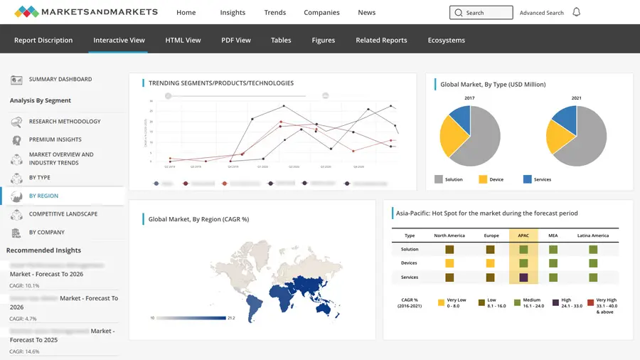
The global semiconductor inspection and metrology market is anticipated to grow from USD 17.31 billion in 2024 to USD 23.30 billion by 2029, growing at a CAGR of 6.1% during the forecast period. Multiple factors are driving the growth of the semiconductor inspection and metrology market. The expanding semiconductor industry, surging adoption of smartphones, laptops, and smart home systems, and rising demand for IoT devices are the key factors that will accelerate the growth of the semiconductor inspection and metrology market during the forecast period. Likewise, the miniaturization of semiconductor devices and integration of AI and ML into semiconductor inspection and metrology equipment is expected to create lucrative opportunities for the semiconductor inspection and metrology market players. However, high setup and operational costs are expected to restrain market growth.


Expanding semiconductor industry
The rising demand for AI applications is fueling the need for advanced chips capable of handling complex computations, while innovations in the automotive sector are increasing the need for semiconductor components. The ongoing global deployment of 5G networks and the proliferation of Internet of Things (IoT) devices are expanding the communication and sensor chips market. Additionally, the recovery of the memory market is restoring balance in the sector, and strategic investments in semiconductor manufacturing capacity ensure supply can meet rising demand. Therefore, the semiconductor industry is set for significant growth, which drives the adoption of semiconductor inspection and metrology equipment. Governments worldwide enforce semiconductor ecosystems by heavily investing in R&D to meet this increasing semiconductor industry.
Wafer inspection system to lead the market during the forecast period
Key features of wafer inspection systems include high throughput capabilities, enabling rapid inspection of multiple wafers without sacrificing accuracy, and advanced imaging techniques like brightfield and darkfield optical inspection for high-resolution defect detection. Additionally, automated analysis features streamline defect classification, while surface analysis ensures that wafers are ready for subsequent processing stages, further improving efficiency and precision in semiconductor production. Therefore, due to the growing instances of surface irregularities and microscopic defects, the wafer inspection system is expected to account for the largest market size during the forecast period.
OSAT companies to register the highest CAGR during the forecast period
OSATs prioritize final quality assurance by implementing inspection and metrology systems that focus on the integrity of packaging and the functional performance of the assembled products. They aim to ensure these products meet stringent quality and functional requirements. To improve efficiency, OSATs frequently employ automated inspection systems, allowing them to effectively handle high volumes of semiconductor devices from various sources. Additionally, these firms must adhere to regulatory compliance, particularly for products intended for critical applications, necessitating robust inspection systems that comprehensively validate the assembled devices. This multifaceted approach enables OSAT companies to maintain high levels of quality while efficiently managing the complexities of semiconductor assembly and testing, which leads to registering the highest CAGR during the forecast period.

Asia Pacific to account for the largest market share during the forecast period
Asia Pacific is expected to have the largest market size during the forecast period. This is attributed to the significant investments in local manufacturing and infrastructure in the region, the high demand for research and development, and the rise in modern industrial technology. Countries like China and South Korea are investing heavily in their semiconductor manufacturing. Meanwhile, major South Korean companies like Samsung and SK Hynix are increasing their demand for advanced metrology solutions to stay competitive. Key players in the semiconductor inspection and metrology market are Applied Materials, Inc. (US), KLA Corporation (US), Hitachi High-Tech Corporation (Japan), ASML (Netherlands), Onto Innovation (US), Nikon Corporation (Japan), NOVA Ltd. (Israel), Camtek (Israel), Thermo Fisher Scientific Inc. (US), and Lasertec Corporation (Japan).
 Exclusive indicates content/data unique to MarketsandMarkets and not available with any competitors.


Growth opportunities and latent adjacency in Semiconductor Inspection and Metrology Market